Clock Generator Module (CGM)
I/O Signals
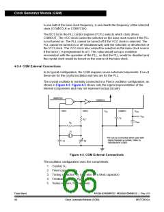
The series resistor (RS) is included in the diagram to follow strict Pierce oscillator
guidelines and may not be required for all ranges of operation, especially with
high-frequency crystals. Refer to the crystal manufacturer’s data for more
information.
Figure 4-3 also shows the external components for the PLL:
•
•
Bypass capacitor, CBYP
Filter capacitor, CF
NOTE:
Routing should be done with great care to minimize signal cross talk and noise.
(See 4.8 Acquisition/Lock Time Specifications for routing information and more
information on the filter capacitor’s value and its effects on PLL performance.)
4.4 I/O Signals
This section describes the CGM input/output (I/O) signals.
4.4.1 Crystal Amplifier Input Pin (OSC1)
The OSC1 pin is an input to the crystal oscillator amplifier.
4.4.2 Crystal Amplifier Output Pin (OSC2)
The OSC2 pin is the output of the crystal oscillator inverting amplifier.
4.4.3 External Filter Capacitor Pin (CGMXFC)
The CGMXFC pin is required by the loop filter to filter out phase corrections. A
small external capacitor is connected to this pin.
NOTE:
To prevent noise problems, CF should be placed as close to the CGMXFC pin as
possible, with minimum routing distances and no routing of other signals across the
CF connection.
4.4.4 PLL Analog Power Pin (VDDA
)
VDDA is a power pin used by the analog portions of the PLL. Connect the VDDA pin
to the same voltage potential as the VDD pin.
NOTE:
Route VDDA carefully for maximum noise immunity and place bypass capacitors as
close as possible to the package.
4.4.5 Oscillator Enable Signal (SIMOSCEN)
The SIMOSCEN signal comes from the system integration module (SIM) and
enables the oscillator and PLL.
MC68HC908MR32 • MC68HC908MR16 — Rev. 6.0
MOTOROLA Clock Generator Module (CGM)
Data Sheet
67

 FREESCALE [ Freescale ]