Clock Generator Module (CGM)
4.4.6 Crystal Output Frequency Signal (CGMXCLK)
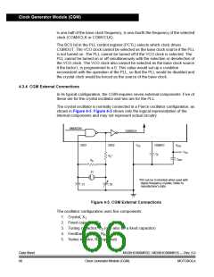
CGMXCLK is the crystal oscillator output signal. It runs at the full speed of the
crystal (fXCLK) and comes directly from the crystal oscillator circuit. Figure 4-3
shows only the logical relation of CGMXCLK to OSC1 and OSC2 and may not
represent the actual circuitry. The duty cycle of CGMXCLK is unknown and may
depend on the crystal and other external factors. Also, the frequency and amplitude
of CGMXCLK can be unstable at startup.
4.4.7 CGM Base Clock Output (CGMOUT)
CGMOUT is the clock output of the CGM. This signal goes to the SIM, which
generates the MCU clocks. CGMOUT is a 50 percent duty cycle clock running at
twice the bus frequency. CGMOUT is software programmable to be either the
oscillator output, CGMXCLK, divided by two or the VCO clock, CGMVCLK, divided
by two.
4.4.8 CGM CPU Interrupt (CGMINT)
CGMINT is the interrupt signal generated by the PLL lock detector.
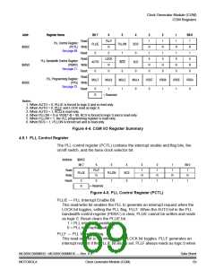
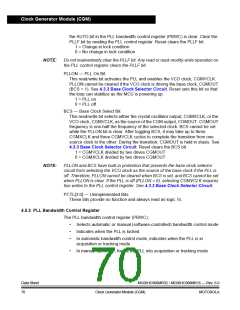
4.5 CGM Registers
These registers control and monitor operation of the CGM:
•
•
PLL control register (PCTL) — see 4.5.1 PLL Control Register
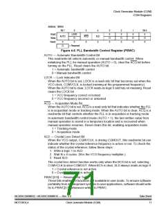
PLL bandwidth control register (PBWC) — see 4.5.2 PLL Bandwidth
Control Register
•
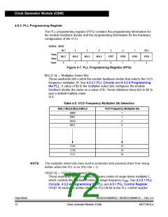
PLL programming register (PPG) — see 4.5.3 PLL Programming Register
Figure 4-4 is a summary of the CGM registers.
Data Sheet
68
MC68HC908MR32 • MC68HC908MR16 — Rev. 6.0
Clock Generator Module (CGM) MOTOROLA

 FREESCALE [ Freescale ]