Clock Generator Module (CGM)
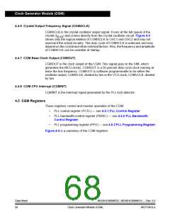
CGM Registers
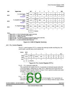
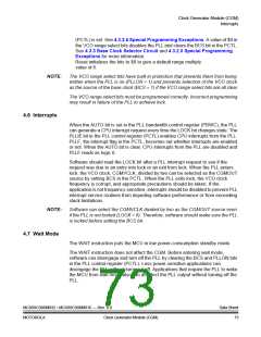
Addr.
Register Name
Bit 7
PLLIE
0
6
PLLF
R
5
PLLON
1
4
BCS
0
3
1
2
1
1
1
Bit 0
Read:
PLL Control Register
(PCTL) Write:
1
R
1
$005C
R
1
R
1
R
1
See page 69.
Reset:
Read:
0
LOCK
R
0
0
0
0
PLL Bandwidth Control Register
AUTO
0
ACQ
0
XLD
0
$005D
$005E
Notes:
(PBWC) Write:
R
0
R
0
R
0
R
0
See page 71.
Reset:
Read:
0
PLL Programming Register
MUL7
MUL6
MUL5
1
MUL4
0
VRS7
0
VRS6
1
VRS5
1
VRS4
0
(PPG) Write:
See page 72.
Reset:
0
1
= Reserved
R
1. When AUTO = 0, PLLIE is forced to logic 0 and is read-only.
2. When AUTO = 0, PLLF and LOCK read as logic 0.
3. When AUTO = 1, ACQ is read-only.
4. When PLLON = 0 or VRS[7:4] = $0, BCS is forced to logic 0 and is read-only.
5. When PLLON = 1, the PLL programming register is read-only.
6. When BCS = 1, PLLON is forced set and is read-only.
Figure 4-4. CGM I/O Register Summary
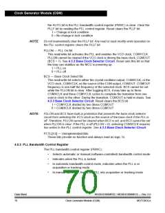
4.5.1 PLL Control Register
The PLL control register (PCTL) contains the interrupt enable and flag bits, the
on/off switch, and the base clock selector bit.
Address:
$005C
Bit 7
6
5
PLLON
1
4
BCS
0
3
1
2
1
1
1
Bit 0
1
Read:
Write:
Reset:
PLLF
PLLIE
R
R
1
R
1
R
1
R
0
0
1
= Reserved
R
Figure 4-5. PLL Control Register (PCTL)
PLLIE — PLL Interrupt Enable Bit
This read/write bit enables the PLL to generate an interrupt request when the
LOCK bit toggles, setting the PLL flag, PLLF. When the AUTO bit in the PLL
bandwidth control register (PBWC) is clear, PLLIE cannot be written and reads
as logic 0. Reset clears the PLLIE bit.
1 = PLL interrupts enabled
0 = PLL interrupts disabled
PLLF — PLL Interrupt Flag
This read-only bit is set whenever the LOCK bit toggles. PLLF generates an
interrupt request if the PLLIE bit also is set. PLLF always reads as logic 0 when
MC68HC908MR32 • MC68HC908MR16 — Rev. 6.0
MOTOROLA Clock Generator Module (CGM)
Data Sheet
69

 FREESCALE [ Freescale ]