Clock Generator Module (CGM)
Functional Description
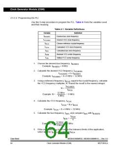
7. Using the value 4.9152 MHz for fNOM, calculate the VCO linear range
multiplier, L. The linear range multiplier controls the frequency range of the
PLL.
fVCLK
fNOM
)
(
L = round
32 MHz
Example: L =
= 7 MHz
4.9152 MHz
8. Calculate the VCO center-of-range frequency, fVRS. The center-or-range
frequency is the midpoint between the minimum and maximum frequencies
attainable by the PLL.
f
VRS = L x fNOM
Example: fVRS = 7 x 4.9152 MHz = 34.4 MHz
For proper operation,
fNOM
fVRS – fVCLK | ≤
2
CAUTION:
Exceeding the recommended maximum bus frequency or VCO frequency can
crash the MCU.
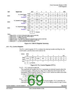
9. Program the PLL registers accordingly:
a. In the upper four bits of the PLL programming register (PPG), program
the binary equivalent of N.
b. In the lower four bits of the PLL programming register (PPG), program
the binary equivalent of L.
4.3.2.5 Special Programming Exceptions
The programming method described in 4.3.2.4 Programming the PLL does not
account for possible exceptions. A value of 0 for N or L is meaningless when used
in the equations given. To account for these exceptions:
•
•
A 0 value for N is interpreted exactly the same as a value of 1.
A 0 value for L disables the PLL and prevents its selection as the source for
the base clock. See 4.3.3 Base Clock Selector Circuit.
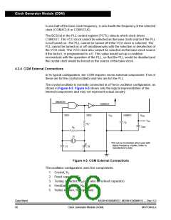
4.3.3 Base Clock Selector Circuit
This circuit is used to select either the crystal clock, CGMXCLK, or the VCO clock,
CGMVCLK, as the source of the base clock, CGMOUT. The two input clocks go
through a transition control circuit that waits up to three CGMXCLK cycles and
three CGMVCLK cycles to change from one clock source to the other. During this
time, CGMOUT is held in stasis. The output of the transition control circuit is then
divided by two to correct the duty cycle. Therefore, the bus clock frequency, which
MC68HC908MR32 • MC68HC908MR16 — Rev. 6.0
MOTOROLA Clock Generator Module (CGM)
Data Sheet
65

 FREESCALE [ Freescale ]