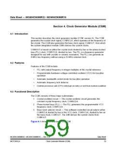
Clock Generator Module (CGM)
Functional Description
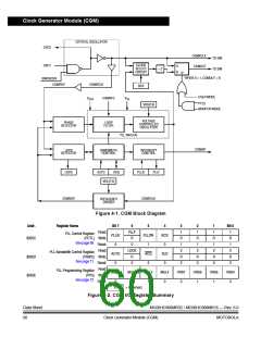
4.3.1 Crystal Oscillator Circuit
The crystal oscillator circuit consists of an inverting amplifier and an external
crystal. The OSC1 pin is the input to the amplifier and the OSC2 pin is the output.
The SIMOSCEN signal from the system integration module (SIM) enables the
crystal oscillator circuit.
The CGMXCLK signal is the output of the crystal oscillator circuit and runs at a rate
equal to the crystal frequency. CGMXCLK is then buffered to produce CGMRCLK,
the PLL reference clock.
CGMXCLK can be used by other modules which require precise timing for
operation. The duty cycle of CGMXCLK is not guaranteed to be 50 percent and
depends on external factors, including the crystal and related external
components.
An externally generated clock also can feed the OSC1 pin of the crystal oscillator
circuit. Connect the external clock to the OSC1 pin and let the OSC2 pin float.
4.3.2 Phase-Locked Loop Circuit (PLL)
The PLL is a frequency generator that can operate in either acquisition mode or
tracking mode, depending on the accuracy of the output frequency. The PLL can
change between acquisition and tracking modes either automatically or manually.
4.3.2.1 PLL Circuits
The PLL consists of these circuits:
•
•
•
•
•
Voltage-controlled oscillator (VCO)
Modulo VCO frequency divider
Phase detector
Loop filter
Lock detector
The operating range of the VCO is programmable for a wide range of frequencies
and for maximum immunity to external noise, including supply and CGMXFC noise.
The VCO frequency is bound to a range from roughly one-half to twice the
center-of-range frequency, fVRS. Modulating the voltage on the CGMXFC pin
changes the frequency within this range. By design, fVRS is equal to the nominal
center-of-range frequency, fNOM, (4.9152 MHz) times a linear factor, L or (L) fNOM
.
CGMRCLK is the PLL reference clock, a buffered version of CGMXCLK.
CGMRCLK runs at a frequency, fRCLK, and is fed to the PLL through a buffer. The
buffer output is the final reference clock, CGMRDV, running at a frequency,
f
RDV = fRCLK.
The VCO’s output clock, CGMVCLK, running at a frequency, fVCLK, is fed back
through a programmable modulo divider. The modulo divider reduces the VCO
MC68HC908MR32 • MC68HC908MR16 — Rev. 6.0
MOTOROLA Clock Generator Module (CGM)
Data Sheet
61

 FREESCALE [ Freescale ]