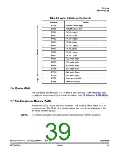
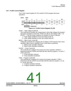
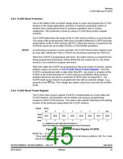
Memory
FLASH Memory (FLASH)
8. Wait for a time, tNVHL (minimum 100 µs).
9. Clear the HVEN bit.
10. After time, tRCV (typical 1 µs), the memory can be accessed in read mode
again.
NOTE:
Programming and erasing of FLASH locations cannot be performed by code being
executed from the FLASH memory. While these operations must be performed in
the order shown, other unrelated operations may occur between the steps.
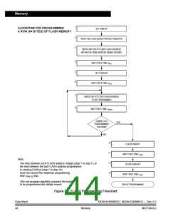
2.8.4 FLASH Program Operation
Use the following step-by-step procedure to program a row of FLASH memory.
Figure 2-4 shows a flowchart of the programming algorithm.
NOTE:
Only bytes which are currently $FF may be programmed.
1. Set the PGM bit. This configures the memory for program operation and
enables the latching of address and data for programming.
2. Read the FLASH block protect register.
3. Write any data to any FLASH location within the address range desired.
4. Wait for a time, tNVS (minimum 10 µs).
5. Set the HVEN bit.
6. Wait for a time, tPGS (minimum 5 µs).
7. Write data to the FLASH address being programmed(1).
8. Wait for time, tPROG (minimum 30 µs).
9. Repeat step 7 and 8 until all desired bytes within the row are programmed.
10. Clear the PGM bit(1).
11. Wait for time, tNVH (minimum 5 µs).
12. Clear the HVEN bit.
13. After time, tRCV (typical 1 µs), the memory can be accessed in read mode
again.
NOTE:
NOTE:
The COP register at location $FFFF should not be written between steps 5-12,
when the HVEN bit is set. Since this register is located at a valid FLASH address,
unpredictable behavior may occur if this location is written while HVEN is set.
This program sequence is repeated throughout the memory until all data is
programmed.
Programming and erasing of FLASH locations cannot be performed by code being
executed from the FLASH memory. While these operations must be performed in
the order shown, other unrelated operations may occur between the steps. Do not
exceed tPROG maximum, see 19.6 FLASH Memory Characteristics.
1. The time between each FLASH address change, or the time between the last FLASH address
programmed to clearing PGM bit, must not exceed the maximum programming time, tPROG
maximum.
MC68HC908MR32 • MC68HC908MR16 — Rev. 6.0
MOTOROLA
Data Sheet
43
Memory

 FREESCALE [ Freescale ]