Memory
FLASH Memory (FLASH)
2.8.5 FLASH Block Protection
Due to the ability of the on-board charge pump to erase and program the FLASH
memory in the target application, provision is made for protecting a block of
memory from unintentional erase or program operations due to system
malfunction. This protection is done by using a FLASH block protect register
(FLBPR).
The FLBPR determines the range of the FLASH memory which is to be protected.
The range of the protected area starts from a location defined by FLBPR and ends
at the bottom of the FLASH memory ($FFFF). When the memory is protected, the
HVEN bit cannot be set in either ERASE or PROGRAM operations.
NOTE:
In performing a program or erase operation, the FLASH block protect register must
be read after setting the PGM or ERASE bit and before asserting the HVEN bit
When the FLBPR is programmed with all 0s, the entire memory is protected from
being programmed and erased. When all the bits are erased (all 1s), the entire
memory is accessible for program and erase.
When bits within the FLBPR are programmed, they lock a block of memory, whose
address ranges are shown in 2.8.6 FLASH Block Protect Register. Once the
FLBPR is programmed with a value other than $FF, any erase or program of the
FLBPR or the protected block of FLASH memory is prohibited. Mass erase is
disabled whenever any block is protected (FLBPR does not equal $FF). The
FLBPR itself can be erased or programmed only with an external voltage, VTST
,
present on the IRQ pin. This voltage also allows entry from reset into the monitor
mode.
2.8.6 FLASH Block Protect Register
The FLASH block protect register (FLBPR) is implemented as a byte within the
FLASH memory, and therefore can be written only during a programming
sequence of the FLASH memory. The value in this register determines the starting
location of the protected range within the FLASH memory.
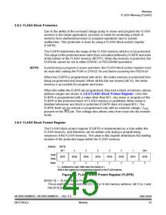
Address:
$FF7E
Bit 7
6
BPR6
0
5
BPR5
0
4
BPR4
0
3
BPR3
0
2
BPR2
0
1
BPR1
0
Bit 0
BPR0
0
Read:
Write:
Reset:
BPR7
0
U = Unaffected by reset. Initial value from factory is 1.
Write to this register by a programming sequence to the FLASH memory.
Figure 2-5. FLASH Block Protect Register (FLBPR)
BPR[7:0] — FLASH Block Protect Bits
These eight bits represent bits [14:7] of a 16-bit memory address. Bit 15 is 1 and
bits [6:0] are 0s.
MC68HC908MR32 • MC68HC908MR16 — Rev. 6.0
MOTOROLA
Data Sheet
45
Memory

 FREESCALE [ Freescale ]