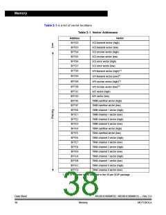
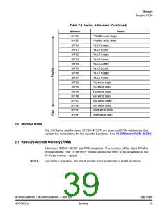
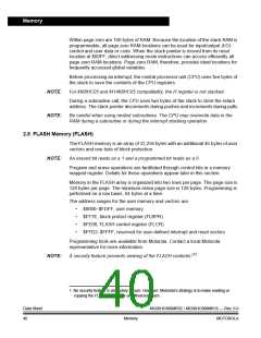
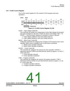
Memory
2.8.2 FLASH Page Erase Operation
Use this step-by-step procedure to erase a page (128 bytes) of FLASH memory.
1. Set the ERASE bit and clear the MASS bit in the FLASH control register.
2. Read the FLASH block protect register.
3. Write any data to any FLASH location within the address range of the block
to be erased.
4. Wait for a time, tNVS (minimum 10 µs).
5. Set the HVEN bit.
6. Wait for a time, tErase (minimum 1 ms or 4 ms).
7. Clear the ERASE bit.
8. Wait for a time, tNVH (minimum 5 µs).
9. Clear the HVEN bit.
10. After time, tRCV (typical 1 µs), the memory can be accessed in read mode
again.
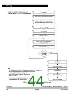
NOTE:
Programming and erasing of FLASH locations cannot be performed by code being
executed from the FLASH memory. While these operations must be performed in
the order shown, other unrelated operations may occur between the steps.
In applications that require more than 1000 program/erase cycles, use the 4 ms
page erase specification to get improved long-term reliability. Any application can
use this 4 ms page erase specification. However, in applications where a FLASH
location will be erased and reprogrammed less than 1000 times, and speed is
important, use the 1 ms page erase specification to get a shorter cycle time.
2.8.3 FLASH Mass Erase Operation
Use this step-by-step procedure to erase the entire FLASH memory.
1. Set both the ERASE bit and the MASS bit in the FLASH control register.
2. Read the FLASH block protect register.
3. Write any data to any FLASH address(1) within the FLASH memory address
range.
4. Wait for a time, tNVS (minimum 10 µs).
5. Set the HVEN bit.
6. Wait for a time, tMErase (minimum 4 ms).
7. Clear the ERASE and MASS bits.
NOTE:
Mass erase is disabled whenever any block is protected (FLBPR does not equal
$FF).
1. When in monitor mode, with security sequence failed (see 18.3.2 Security), write to the FLASH
block protect register instead of any FLASH address.
Data Sheet
42
MC68HC908MR32 • MC68HC908MR16 — Rev. 6.0
Memory
MOTOROLA

 FREESCALE [ Freescale ]