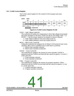
Memory
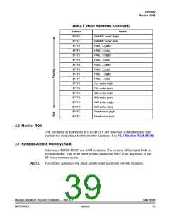
Within page zero are 160 bytes of RAM. Because the location of the stack RAM is
programmable, all page zero RAM locations can be used for input/output (I/O)
control and user data or code. When the stack pointer is moved from its reset
location at $00FF, direct addressing mode instructions can access efficiently all
page zero RAM locations. Page zero RAM, therefore, provides ideal locations for
frequently accessed global variables.
Before processing an interrupt, the central processor unit (CPU) uses five bytes of
the stack to save the contents of the CPU registers.
NOTE:
NOTE:
For M68HC05 and M1468HC05 compatibility, the H register is not stacked.
During a subroutine call, the CPU uses two bytes of the stack to store the return
address. The stack pointer decrements during pushes and increments during pulls.
Be careful when using nested subroutines. The CPU may overwrite data in the
RAM during a subroutine or during the interrupt stacking operation.
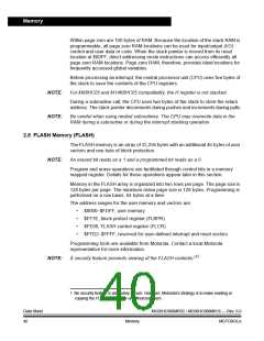
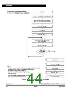
2.8 FLASH Memory (FLASH)
The FLASH memory is an array of 32,256 bytes with an additional 46 bytes of user
vectors and one byte of block protection.
NOTE:
An erased bit reads as a 1 and a programmed bit reads as a 0.
Program and erase operations are facilitated through control bits in a memory
mapped register. Details for these operations appear later in this section.
Memory in the FLASH array is organized into two rows per page. The page size is
128 bytes per page. The minimum erase page size is 128 bytes. Programming is
performed on a row basis, 64 bytes at a time.
The address ranges for the user memory and vectors are:
•
•
•
•
$8000–$FDFF, user memory
$FF7E, block protect register (FLBPR)
$FE08, FLASH control register (FLCR)
$FFD2–$FFFF, reserved for user-defined interrupt and reset vectors
Programming tools are available from Motorola. Contact a local Motorola
representative for more information.
NOTE:
A security feature prevents viewing of the FLASH contents.(1)
1. No security feature is absolutely secure. However, Motorola’s strategy is to make reading or
copying the FLASH difficult for unauthorized users.
Data Sheet
40
MC68HC908MR32 • MC68HC908MR16 — Rev. 6.0
Memory
MOTOROLA

 FREESCALE [ Freescale ]