Timer Interface B (TIMB)
I/O Registers
PTE0/TCLKB is available as a general-purpose I/O pin or ADC channel when not
used as the TIMB clock input. When the PTE0/TCLKB pin is the TIMB clock input,
it is an input regardless of the state of the DDRE0 bit in data direction register E.
17.6.2 TIMB Channel I/O Pins (PTE1/TCH0B–PTE2/TCH1B)
Each channel I/O pin is programmable independently as an input capture pin or an
output compare pin. PTE1/TCH0B and PTE2/TCH1B can be configured as
buffered output compare or buffered PWM pins.
17.7 I/O Registers
These input/output (I/O) registers control and monitor TIMB operation:
•
•
•
•
•
TIMB status and control register (TBSC)
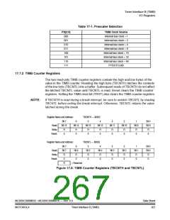
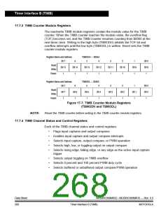
TIMB control registers (TBCNTH–TBCNTL)
TIMB counter modulo registers (TBMODH–TBMODL)
TIMB channel status and control registers (TBSC0 and TBSC1)
TIMB channel registers (TBCH0H–TBCH0L and TBCH1H–TBCH1L)
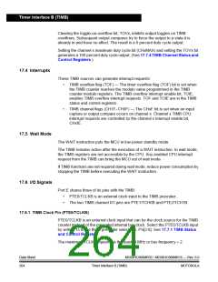
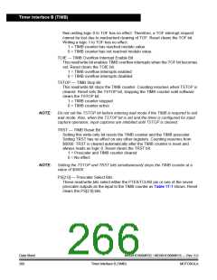
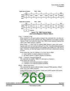
17.7.1 TIMB Status and Control Register
The TIMB status and control register:
•
•
•
•
•
Enables TIMB overflow interrupts
Flags TIMB overflows
Stops the TIMB counter
Resets the TIMB counter
Prescales the TIMB counter clock
Address:
$0051
Bit 7
TOF
0
6
5
TSTOP
1
4
0
3
0
2
PS2
0
1
PS1
0
Bit 0
PS0
0
Read:
Write:
Reset:
TOIE
TRST
0
R
0
0
0
R
= Reserved
Figure 17-5. TIMB Status and Control Register (TBSC)
TOF — TIMB Overflow Flag
This read/write flag is set when the TIMB counter reaches the modulo value
programmed in the TIMB counter modulo registers. Clear TOF by reading the
TIMB status and control register when TOF is set and then writing a logic 0 to
TOF. If another TIMB overflow occurs before the clearing sequence is complete,
MC68HC908MR32 • MC68HC908MR16 — Rev. 6.0
MOTOROLA Timer Interface B (TIMB)
Data Sheet
265

 FREESCALE [ Freescale ]