Timer Interface B (TIMB)
Functional Description
register (TBSC1) is unused. While the MS0B bit is set, the channel 1 pin,
PTE2/TCH1B, is available as a general-purpose I/O pin.
NOTE:
In buffered PWM signal generation, do not write new pulse width values to the
currently active channel registers. User software should track the currently active
channel to prevent writing a new value to the active channel. Writing to the active
channel registers is the same as generating unbuffered PWM signals.
17.3.4.3 PWM Initialization
To ensure correct operation when generating unbuffered or buffered PWM signals,
use this initialization procedure:
1. In the TIMB status and control register (TBSC):
a. Stop the TIMB counter by setting the TIMB stop bit, TSTOP.
b. Reset the TIMB counter and prescaler by setting the TIMB reset bit,
TRST.
2. In the TIMB counter modulo registers (TBMODH–TBMODL), write the value
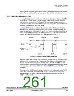
for the required PWM period.
3. In the TIMB channel x registers (TBCHxH–TBCHxL), write the value for the
required pulse width.
4. In TIMB channel x status and control register (TBSCx):
a. Write 0:1 (for unbuffered output compare or PWM signals) or 1:0 (for
buffered output compare or PWM signals) to the mode select bits,
MSxB–MSxA. (See Table 17-2.)
b. Write 1 to the toggle-on-overflow bit, TOVx.
c. Write 1:0 (polarity 1 — to clear output on compare) or 1:1 (polarity 0 —
to set output on compare) to the edge/level select bits, ELSxB–ELSxA.
The output action on compare must force the output to the complement
of the pulse width level. (See Table 17-2.)
NOTE:
In PWM signal generation, do not program the PWM channel to toggle on output
compare. Toggling on output compare prevents reliable 0 percent duty cycle
generation and removes the ability of the channel to self-correct in the event of
software error or noise. Toggling on output compare can also cause incorrect PWM
signal generation when changing the PWM pulse width to a new, much larger
value.
5. In the TIMB status control register (TBSC), clear the TIMB stop bit, TSTOP.
Setting MS0B links channels 0 and 1 and configures them for buffered PWM
operation. The TIMB channel 0 registers (TBCH0H–TBCH0L) initially control the
buffered PWM output. TIMB status control register 0 (TBSC0) controls and
monitors the PWM signal from the linked channels. MS0B takes priority over
MS0A.
MC68HC908MR32 • MC68HC908MR16 — Rev. 6.0
MOTOROLA
Data Sheet
263
Timer Interface B (TIMB)

 FREESCALE [ Freescale ]