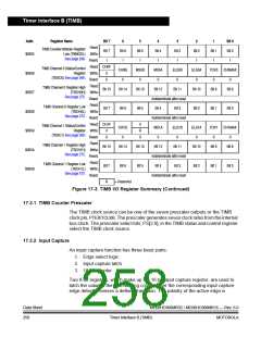
Timer Interface B (TIMB)
17.3.4.1 Unbuffered PWM Signal Generation
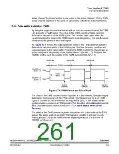
Any output compare channel can generate unbuffered PWM pulses as described
in 17.3.4 Pulse-Width Modulation (PWM). The pulses are unbuffered because
changing the pulse width requires writing the new pulse width value over the value
currently in the TIMB channel registers.
An unsynchronized write to the TIMB channel registers to change a pulse width
value could cause incorrect operation for up to two PWM periods. For example,
writing a new value before the counter reaches the old value but after the counter
reaches the new value prevents any compare during that PWM period. Also, using
a TIMB overflow interrupt routine to write a new, smaller pulse width value may
cause the compare to be missed. The TIMB may pass the new value before it is
written to the TIMB channel registers.
Use this method to synchronize unbuffered changes in the PWM pulse width on
channel x:
•
•
When changing to a shorter pulse width, enable channel x output compare
interrupts and write the new value in the output compare interrupt routine.
The output compare interrupt occurs at the end of the current pulse. The
interrupt routine has until the end of the PWM period to write the new value.
When changing to a longer pulse width, enable TIMB overflow interrupts and
write the new value in the TIMB overflow interrupt routine. The TIMB
overflow interrupt occurs at the end of the current PWM period. Writing a
larger value in an output compare interrupt routine (at the end of the current
pulse) could cause two output compares to occur in the same PWM period.
NOTE:
In PWM signal generation, do not program the PWM channel to toggle on output
compare. Toggling on output compare prevents reliable 0 percent duty cycle
generation and removes the ability of the channel to self-correct in the event of
software error or noise. Toggling on output compare also can cause incorrect PWM
signal generation when changing the PWM pulse width to a new, much larger
value.
17.3.4.2 Buffered PWM Signal Generation
Channels 0 and 1 can be linked to form a buffered PWM channel whose output
appears on the PTE1/TCH0B pin. The TIMB channel registers of the linked pair
alternately control the pulse width of the output.
Setting the MS0B bit in TIMB channel 0 status and control register (TBSC0) links
channel 0 and channel 1. The TIMB channel 0 registers initially control the pulse
width on the PTE1/TCH0B pin. Writing to the TIMB channel 1 registers enables the
TIMB channel 1 registers to synchronously control the pulse width at the beginning
of the next PWM period. At each subsequent overflow, the TIMB channel registers
(0 or 1) that control the pulse width are the ones written to last. TBSC0 controls and
monitors the buffered PWM function, and TIMB channel 1 status and control
Data Sheet
262
MC68HC908MR32 • MC68HC908MR16 — Rev. 6.0
Timer Interface B (TIMB)
MOTOROLA

 FREESCALE [ Freescale ]