Timer Interface A (TIMA)
I/O Registers
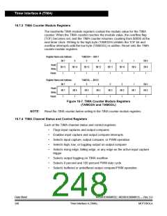
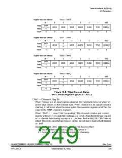
Register Name and Address:
Bit 7
TASC0 — $0013
5
6
CH0IE
0
4
3
ELS0B
0
2
ELS0A
0
1
TOV0
0
Bit 0
CH0MAX
0
Read:
Write:
Reset:
CH0F
MS0B
0
MS0A
0
0
0
Register Name and Address:
Bit 7
TASC1 — $0016
6
CH1IE
0
5
0
4
3
ELS1B
0
2
ELS1A
0
1
TOV1
0
Bit 0
CH1MAX
0
Read:
Write:
Reset:
CH1F
MS1A
0
0
0
R
0
Register Name and Address:
Bit 7
TASC2 — $0019
5
6
CH2IE
0
4
3
ELS2B
0
2
ELS2A
0
1
TOV2
0
Bit 0
CH2MAX
0
Read:
Write:
Reset:
CH2F
MS2B
0
MS2A
0
0
0
Register Name and Address:
Bit 7
TASC3 — $001C
6
5
0
4
3
ELS3B
0
2
ELS3A
0
1
TOV3
0
Bit 0
CH3MAX
0
Read:
Write:
Reset:
CH3F
CH3IE
MS3A
0
0
0
R
0
0
R
= Reserved
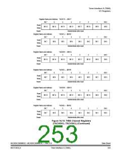
Figure 16-8. TIMA Channel Status
and Control Registers (TASC0–TASC3)
CHxF — Channel x Flag Bit
When channel x is an input capture channel, this read/write bit is set when an
active edge occurs on the channel x pin. When channel x is an output compare
channel, CHxF is set when the value in the TIMA counter registers matches the
value in the TIMA channel x registers.
When CHxIE = 1, clear CHxF by reading TIMA channel x status and control
register with CHxF set, and then writing a 0 to CHxF. If another interrupt request
occurs before the clearing sequence is complete, then writing 0 to CHxF has no
effect. Therefore, an interrupt request cannot be lost due to inadvertent clearing
of CHxF.
Reset clears the CHxF bit. Writing a 1 to CHxF has no effect.
1 = Input capture or output compare on channel x
0 = No input capture or output compare on channel x
MC68HC908MR32 • MC68HC908MR16 — Rev. 6.0
MOTOROLA Timer Interface A (TIMA)
Data Sheet
249

 FREESCALE [ Freescale ]