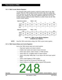
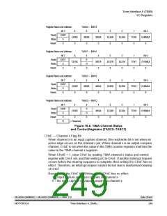
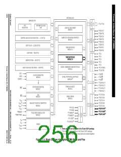
Timer Interface A (TIMA)
OVERFLOW
OVERFLOW
OVERFLOW
OVERFLOW
OVERFLOW
PERIOD
PTEx/TCHx
OUTPUT
COMPARE
OUTPUT
COMPARE
OUTPUT
COMPARE
OUTPUT
COMPARE
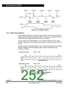
CHxMAX
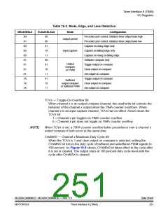
TOVx
Figure 16-9. CHxMAX Latency
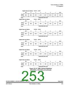
16.7.5 TIMA Channel Registers
These read/write registers contain the captured TIMA counter value of the input
capture function or the output compare value of the output compare function. The
state of the TIMA channel registers after reset is unknown.
In input capture mode (MSxB:MSxA = 0:0), reading the high byte of the TIMA
channel x registers (TACHxH) inhibits input captures until the low byte (TACHxL)
is read.
In output compare mode (MSxB:MSxA ≠ 0:0), writing to the high byte of the TIMA
channel x registers (TACHxH) inhibits output compares until the low byte
(TACHxL) is written.
Register Name and Address:
TACH0H — $0014
Bit 7
6
5
4
3
2
1
Bit 0
Bit 8
Read:
Bit 15
Write:
Bit 14
Bit 13
Bit 12
Bit 11
Bit 10
Bit 9
Reset:
Indeterminate after reset
Register Name and Address:
Bit 7
TACH0L — $0015
6
5
4
3
2
1
Bit 0
Bit 0
Read:
Bit 7
Write:
Bit 6
Bit 5
Bit 4
Bit 3
Bit 2
Bit 1
Reset:
Indeterminate after reset
Figure 16-10. TIMA Channel Registers
(TACH0H/L–TACH3H/L)
Data Sheet
252
MC68HC908MR32 • MC68HC908MR16 — Rev. 6.0
MOTOROLA
Timer Interface A (TIMA)

 FREESCALE [ Freescale ]