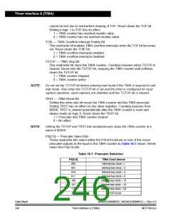
Timer Interface A (TIMA)
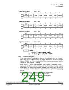
CHxIE — Channel x Interrupt Enable Bit
This read/write bit enables TIMA CPU interrupts on channel x.
Reset clears the CHxIE bit.
1 = Channel x CPU interrupt requests enabled
0 = Channel x CPU interrupt requests disabled
MSxB — Mode Select Bit B
This read/write bit selects buffered output compare/PWM operation. MSxB
exists only in the TIMA channel 0 and TIMA channel 2 status and control
registers.
Setting MS0B disables the channel 1 status and control register and reverts
TCH1A pin to general-purpose I/O.
Setting MS2B disables the channel 3 status and control register and reverts
TCH3A pin to general-purpose I/O.
Reset clears the MSxB bit.
1 = Buffered output compare/PWM operation enabled
0 = Buffered output compare/PWM operation disabled
MSxA — Mode Select Bit A
When ELSxB:A ≠ 00, this read/write bit selects either input capture operation or
unbuffered output compare/PWM operation. See Table 16-2.
1 = Unbuffered output compare/PWM operation
0 = Input capture operation
When ELSxB:A = 00, this read/write bit selects the initial output level of the
TCHxA pin once PWM, input capture, or output compare operation is enabled.
See Table 16-2. Reset clears the MSxA bit.
1 = Initial output level low
0 = Initial output level high
NOTE:
Before changing a channel function by writing to the MSxB or MSxA bit, set the
TSTOP and TRST bits in the TIMA status and control register (TASC).
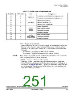
ELSxB and ELSxA — Edge/Level Select Bits
When channel x is an input capture channel, these read/write bits control the
active edge-sensing logic on channel x.
When channel x is an output compare channel, ELSxB and ELSxA control the
channel x output behavior when an output compare occurs.
When ELSxB and ELSxA are both clear, channel x is not connected to port E,
and pin PTEx/TCHxA is available as a general-purpose I/O pin. However,
channel x is at a state determined by these bits and becomes transparent to the
respective pin when PWM, input capture, or output compare mode is enabled.
Table 16-2 shows how ELSxB and ELSxA work. Reset clears the ELSxB and
ELSxA bits.
NOTE:
Before enabling a TIMA channel register for input capture operation, make sure
that the PTEx/TACHx pin is stable for at least two bus clocks.
Data Sheet
250
MC68HC908MR32 • MC68HC908MR16 — Rev. 6.0
Timer Interface A (TIMA)
MOTOROLA

 FREESCALE [ Freescale ]