Timer Interface A (TIMA)
I/O Registers
16.6.2 TIMA Channel I/O Pins (PTE4/TCH0A–PTE7/TCH3A)
Each channel I/O pin is programmable independently as an input capture pin or an
output compare pin. PTE2/TCH0 and PTE4/TCH2 can be configured as buffered
output compare or buffered PWM pins.
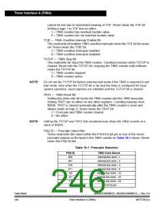
16.7 I/O Registers
These input/output (I/O) registers control and monitor TIMA operation:
•
•
•
•
TIMA status and control register (TASC)
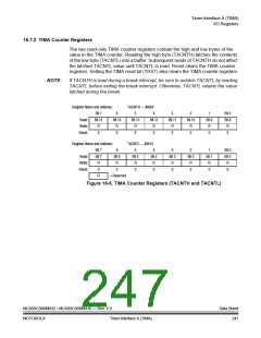
TIMA control registers (TACNTH–TACNTL)
TIMA counter modulo registers (TAMODH–TAMODL)
TIMA channel status and control registers (TASC0, TASC1, TASC2, and
TASC3)
•
TIMA channel registers (TACH0H–TACH0L, TACH1H–TACH1L,
TACH2H–TACH2L, and TACH3H–TACH3L)
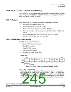
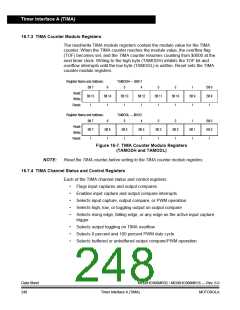
16.7.1 TIMA Status and Control Register
The TIMA status and control register:
•
•
•
•
•
Enables TIMA overflow interrupts
Flags TIMA overflows
Stops the TIMA counter
Resets the TIMA counter
Prescales the TIMA counter clock
Address: $000E
Bit 7
6
5
TSTOP
1
4
0
3
0
2
PS2
0
1
PS1
0
Bit 0
PS0
0
Read:
Write:
Reset:
TOF
0
TOIE
TRST
0
R
0
0
0
R
= Reserved
Figure 16-5. TIMA Status and Control Register (TASC)
TOF — TIMA Overflow Flag
This read/write flag is set when the TIMA counter reaches the modulo value
programmed in the TIMA counter modulo registers. Clear TOF by reading the
TIMA status and control register when TOF is set and then writing a logic 0 to
TOF. If another TIMA overflow occurs before the clearing sequence is complete,
then writing logic 0 to TOF has no effect. Therefore, a TOF interrupt request
MC68HC908MR32 • MC68HC908MR16 — Rev. 6.0
MOTOROLA Timer Interface A (TIMA)
Data Sheet
245

 FREESCALE [ Freescale ]