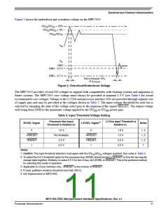
Electrical and Thermal Characteristics
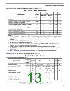
Table 5 provides the package thermal characteristics for the MPC7455.
6
Table 5. Package Thermal Characteristics
Value
Characteristic
Symbol
Unit
Notes
MPC7445
MPC7455
Junction-to-ambient thermal resistance, natural
convection
R
22
20
°C/W
°C/W
°C/W
°C/W
1, 2
1, 3
1, 3
1, 3
JA
θ
Junction-to-ambient thermal resistance, natural
convection, four-layer (2s2p) board
R
14
16
11
14
15
11
JMA
JMA
JMA
θ
θ
θ
Junction-to-ambient thermal resistance, 200 ft/min
airflow, single-layer (1s) board
R
R
Junction-to-ambient thermal resistance, 200 ft/min
airflow, four-layer (2s2p) board
Junction-to-board thermal resistance
Junction-to-case thermal resistance
Notes:
R
6
6
°C/W
°C/W
4
5
JB
JC
θ
R
<0.1
<0.1
θ
1. Junction temperature is a function of on-chip power dissipation, package thermal resistance, mounting site (board)
temperature, ambient temperature, airflow, power dissipation of other components on the board, and board thermal
resistance.
2. Per SEMI G38-87 and JEDEC JESD51-2 with the single-layer board horizontal.
3. Per JEDEC JESD51-6 with the board horizontal.
4. Thermal resistance between the die and the printed-circuit board per JEDEC JESD51-8. Board temperature is
measured on the top surface of the board near the package.
5. Thermal resistance between the die and the case top surface as measured by the cold plate method
(MIL SPEC-883 Method 1012.1) with the calculated case temperature. The actual value of R
than 0.1°C/W.
for the part is less
θJC
6. Refer to Section 9.8, “Thermal Management Information,” for more details about thermal management.
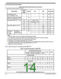
Table 6 provides the DC electrical characteristics for the MPC7455.
Table 6. DC Electrical Specifications
At recommended operating conditions. See Table 4.
Nominal
Characteristic
Bus
Voltage
Symbol
Min
Max
Unit Notes
1
Input high voltage
1.5
1.8
2.5
1.5
1.8
2.5
—
V
GV × 0.65
GV + 0.3
V
V
V
V
V
V
V
V
6
IH
DD
DD
(all inputs except SYSCLK)
V
OV /GV × 0.65 OV /GV + 0.3
DD DD DD DD
IH
V
1.7
OV /GV + 0.3
DD DD
IH
Input low voltage
V
V
V
–0.3
–0.3
–0.3
1.4
GV × 0.35
6
IL
IL
IL
DD
(all inputs except SYSCLK)
OV /GV × 0.35
DD
DD
0.7
SYSCLK input high voltage
SYSCLK input low voltage
CV
OV + 0.3
IH
DD
—
CV
–0.3
0.4
IL
MPC7455 RISC Microprocessor Hardware Specifications, Rev. 4.1
Freescale Semiconductor
13

 FREESCALE [ Freescale ]