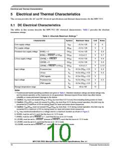
Electrical and Thermal Characteristics
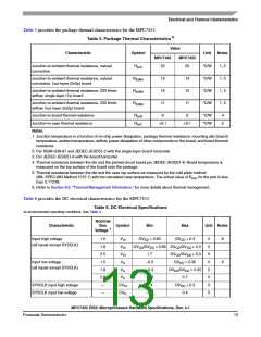
Table 4 provides the recommended operating conditions for the MPC7455.
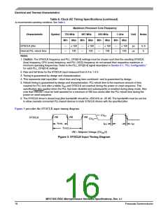
1
Table 4. Recommended Operating Conditions
Recommended Value
Min Max
1.3 V 50 mV
Characteristic
Symbol
Unit
Notes
Core supply voltage
PLL supply voltage
V
V
V
V
V
V
V
V
V
V
V
°C
DD
AV
1.3 V 50 mV
1.8 V 5%
2.5 V 5%
1.8 V 5%
2.5 V 5%
1.5 V 5%
2
DD
Processor bus supply voltage BVSEL = 0
BVSEL = HRESET or OV
OV
OV
GV
GV
GV
DD
DD
DD
DD
DD
in
DD
L3 bus supply voltage
L3VSEL = 0
L3VSEL = HRESET or GV
L3VSEL = ¬HRESET
Processor bus
DD
Input voltage
V
V
V
GND
GND
GND
0
OV
GV
OV
DD
DD
DD
L3 bus
in
JTAG signals
in
Die-junction temperature
T
105
j
Notes:
1. These are the recommended and tested operating conditions. Proper device operation outside of these conditions
is not guaranteed.
2. This voltage is the input to the filter discussed in Section 9.2, “PLL Power Supply Filtering,” and not necessarily the
voltage at the AV pin which may be reduced from V by the filter.
DD
DD
MPC7455 RISC Microprocessor Hardware Specifications, Rev. 4.1
12
Freescale Semiconductor

 FREESCALE [ Freescale ]