Electrical and Thermal Characteristics
5 Electrical and Thermal Characteristics
This section provides the AC and DC electrical specifications and thermal characteristics for the MPC7455.
5.1 DC Electrical Characteristics
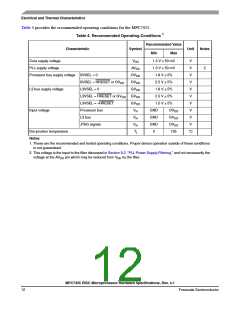
The tables in this section describe the MPC7455 DC electrical characteristics. Table 2 provides the absolute
maximum ratings.
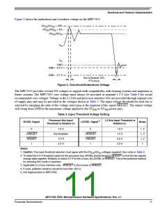
1
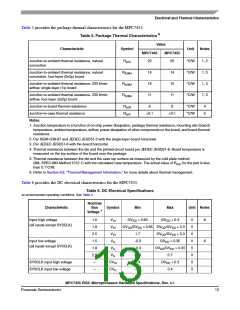
Table 2. Absolute Maximum Ratings
Characteristic
Symbol
Maximum Value
Unit
Notes
Core supply voltage
PLL supply voltage
V
–0.3 to 1.95
–0.3 to 1.95
–0.3 to 1.95
–0.3 to 2.7
–0.3 to 1.65
–0.3 to 1.95
–0.3 to 2.7
V
V
V
V
V
V
V
V
V
V
V
V
°C
4
DD
AV
4
DD
Processor bus supply voltage BVSEL = 0
BVSEL = HRESET or OV
OV
OV
GV
GV
GV
3, 6
3, 7
3, 8
3, 9
3, 10
2, 5
2, 5
DD
DD
DD
DD
DD
in
DD
L3 bus supply voltage
L3VSEL = ¬HRESET
L3VSEL = 0
L3VSEL = HRESET or GV
Processor bus
L3 bus
DD
Input voltage
V
V
V
V
V
–0.3 to OV + 0.3
DD
–0.3 to GV + 0.3
in
DD
JTAG signals
–0.3 to OV + 0.3
DD
in
Input voltage
Processor bus
JTAG signals
–0.3 to OV + 0.3
2, 5
in
DD
–0.3 to OV + 0.3
in
DD
Storage temperature range
T
–55 to 150
stg
Notes:
1. Functional and tested operating conditions are given in Table 4. Absolute maximum ratings are stress ratings only,
and functional operation at the maximums is not guaranteed. Stresses beyond those listed may affect device
reliability or cause permanent damage to the device.
2. Caution: V must not exceed OV or GV by more than 0.3 V at any time including during power-on reset.
in
DD
DD
3. Caution: OV /GV must not exceed V /AV by more than 2.0 V during normal operation; this limit may be
DD
DD
DD
DD
exceeded for a maximum of 20 ms during power-on reset and power-down sequences.
4. Caution: V /AV must not exceed OV /GV by more than 1.0 V during normal operation; this limit may be
DD
DD
DD
DD
exceeded for a maximum of 20 ms during power-on reset and power-down sequences.
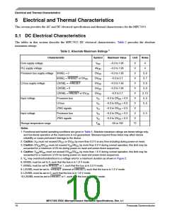
5. V may overshoot/undershoot to a voltage and for a maximum duration as shown in Figure 2.
in
6. BVSEL must be set to 0, such that the bus is in 1.8 V mode.
7. BVSEL must be set to HRESET or 1, such that the bus is in 2.5 V mode.
8. L3VSEL must be set to ¬HRESET (inverse of HRESET), such that the bus is in 1.5 V mode.
9. L3VSEL must be set to 0, such that the bus is in 1.8 V mode.
10.L3VSEL must be set to HRESET or 1, such that the bus is in 2.5 V mode.
MPC7455 RISC Microprocessor Hardware Specifications, Rev. 4.1
10
Freescale Semiconductor

 FREESCALE [ Freescale ]