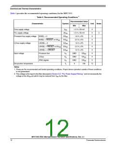
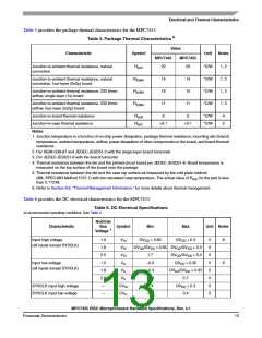
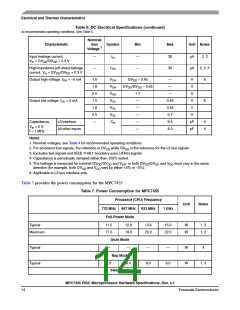
Electrical and Thermal Characteristics
Table 8. Clock AC Timing Specifications (continued)
At recommended operating conditions. See Table 4.
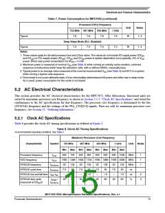
Maximum Processor Core Frequency
733 MHz 867 MHz 933 MHz 1 GHz
Min Max Min Max Min Max
Characteristic
Symbol
Unit
Notes
Min
Max
SYSCLK jitter
—
—
150
100
—
—
150
100
—
—
150
100
—
—
150
100
ps
4, 6
5
Internal PLL relock time
µs
Notes:
1. Caution: The SYSCLK frequency and PLL_CFG[0:4] settings must be chosen such that the resulting SYSCLK
(bus) frequency, CPU (core) frequency, and PLL (VCO) frequency do not exceed their respective maximum or
minimum operating frequencies. Refer to the PLL_CFG[0:4] signal description in Section 9.1, “PLL Configuration,”
for valid PLL_CFG[0:4] settings.
2. Rise and fall times for the SYSCLK input measured from 0.4 to 1.4 V.
3. Timing is guaranteed by design and characterization.
4. This represents total input jitter—short term and long term combined—and is guaranteed by design.
5. Relock timing is guaranteed by design and characterization. PLL-relock time is the maximum amount of time
required for PLL lock after a stable V and SYSCLK are reached during the power-on reset sequence. This
DD
specification also applies when the PLL has been disabled and subsequently re-enabled during sleep mode. Also
note that HRESET must be held asserted for a minimum of 255 bus clocks after the PLL-relock time during the
power-on reset sequence.
6. The SYSCLK driver’s closed loop jitter bandwidth should be <500 kHz at –20 dB. The bandwidth must be set low
to allow cascade connected PLL-based devices to track SYSCLK drivers with the specified jitter.
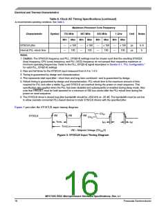
Figure 3 provides the SYSCLK input timing diagram.
CV
t
IH
VM
t
VM
VM
SYSCLK
CV
IL
t
KHKL
KR
KF
t
SYSCLK
VM = Midpoint Voltage (OV /2)
DD
Figure 3. SYSCLK Input Timing Diagram
MPC7455 RISC Microprocessor Hardware Specifications, Rev. 4.1
16
Freescale Semiconductor

 FREESCALE [ Freescale ]