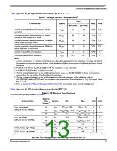
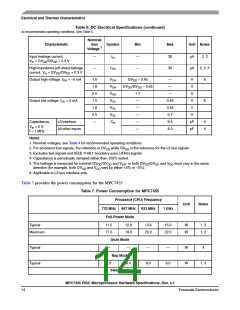
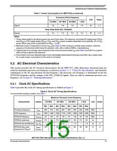
Electrical and Thermal Characteristics
5.2.2 Processor Bus AC Specifications
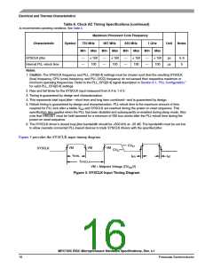
Table 9 provides the processor bus AC timing specifications for the MPC7455 as defined in Figure 4 and Figure 5.
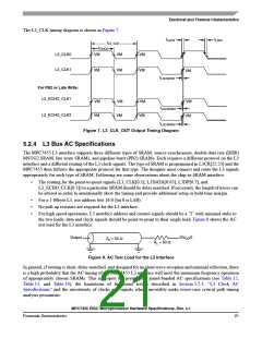
Timing specifications for the L3 bus are provided in Section 5.2.3, “L3 Clock AC Specifications.”
1
Table 9. Processor Bus AC Timing Specifications
At recommended operating conditions. See Table 4.
All Speed Grades
2
Parameter
Symbol
Unit
Notes
Min
Max
Input setup times:
ns
t
2.0
2.0
—
—
A[0:35], AP[0:4], GBL, TBST, TSIZ[0:2], TT[0:3], D[0:63],
DP[0:7]
AVKH
t
IVKH
AACK, ARTRY, BG, CKSTP_IN, DBG, DTI[0:3], QACK, TA,
TBEN, TEA, TS, EXT_QUAL, PMON_IN, SHD[0:1]
BMODE[0:1], BVSEL, L3VSEL
t
2.0
—
8
8
MVKH
Input hold times:
ns
ns
ns
t
0
0
—
—
A[0:35], AP[0:4], GBL, TBST, TSIZ[0:2], TT[0:3], D[0:63],
DP[0:7]
AXKH
t
IXKH
AACK, ARTRY, BG, CKSTP_IN, DBG, DTI[0:3], QACK, TA,
TBEN, TEA, TS,EXT_QUAL, PMON_IN, SHD[0:1]
BMODE[0:1], BVSEL, L3VSEL
t
0
—
MXKH
Output valid times:
t
—
—
—
—
—
2.5
2.5
2.5
2.5
2.5
A[0:35], AP[0:4], GBL, TBST, TSIZ[0:2], TT[0:3], WT, CI
KHAV
t
KHTSV
TS
t
KHDV
D[0:63], DP[0:7]
t
KHARV
ARTRY/SHD0/SHD1
t
KHOV
BR, CKSTP_OUT, DRDY, HIT, PMON_OUT, QREQ]
Output hold times:
t
0.5
0.5
0.5
0.5
0.5
—
—
—
—
—
A[0:35], AP[0:4], GBL, TBST, TSIZ[0:2], TT[0:3], WT, CI
KHAX
t
KHTSX
TS
t
KHDX
D[0:63], DP[0:7]
t
KHARX
ARTRY/SHD0/SHD1
t
KHOX
BR, CKSTP_OUT, DRDY, HIT, PMON_OUT, QREQ
SYSCLK to output enable
t
0.5
—
—
ns
ns
KHOE
SYSCLK to output high impedance (all except TS, ARTRY,
SHD0, SHD1)
t
3.5
KHOZ
SYSCLK to TS high impedance after precharge
Maximum delay to ARTRY/SHD0/SHD1 precharge
t
—
—
1
1
t
t
3, 4, 5
KHTSPZ
SYSCLK
t
3, 5,
6, 7
KHARP
SYSCLK
MPC7455 RISC Microprocessor Hardware Specifications, Rev. 4.1
Freescale Semiconductor
17

 FREESCALE [ Freescale ]