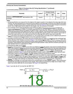
Electrical and Thermal Characteristics
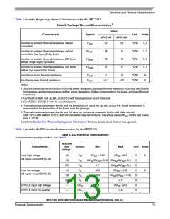
Table 6. DC Electrical Specifications (continued)
At recommended operating conditions. See Table 4.
Nominal
Characteristic
Bus
Voltage
Symbol
Min
Max
Unit Notes
1
Input leakage current,
—
I
—
—
30
30
µA
µA
2, 3
2, 3, 5
6
in
V
= GV /OV + 0.3 V
in
DD DD
High impedance (off-state) leakage
current, V = GV /OV + 0.3 V
—
I
TSI
in
DD
DD
Output high voltage, I
= –5 mA
1.5
1.8
2.5
1.5
1.8
2.5
—
V
V
V
GV – 0.45
—
—
V
V
OH
OH
OH
OH
DD
OV /GV – 0.45
DD
DD
1.7
—
V
Output low voltage, I = 5 mA
V
V
V
—
—
—
—
—
0.45
0.45
0.7
9.5
8.0
V
6
OL
OL
OL
OL
V
V
Capacitance,
= 0 V,
f = 1 MHz
L3 interface
C
pF
pF
4
4
in
V
in
All other inputs
Notes:
1. Nominal voltages; see Table 4 for recommended operating conditions.
2. For processor bus signals, the reference is OV while GV is the reference for the L3 bus signals.
DD
DD
3. Excludes test signals and IEEE 1149.1 boundary scan (JTAG) signals.
4. Capacitance is periodically sampled rather than 100% tested.
5. The leakage is measured for nominal OV /GV and V , or both OV /GV and V must vary in the same
DD
DD
DD
DD
DD
DD
direction (for example, both OV and V vary by either +5% or –5%).
DD
DD
6. Applicable to L3 bus interface only.
Table 7 provides the power consumption for the MPC7455.
Table 7. Power Consumption for MPC7455
Processor (CPU) Frequency
Unit
Notes
733 MHz
867 MHz
933 MHz
1 GHz
Full-Power Mode
Typical
11.5
17.0
12.9
19.0
13.6
20.0
15.0
22.0
W
W
1, 3
1, 2
Maximum
Doze Mode
Typical
Typical
—
—
—
—
W
W
4
Nap Mode
8.0
8.0
8.0
8.0
1, 3
Sleep Mode
MPC7455 RISC Microprocessor Hardware Specifications, Rev. 4.1
14
Freescale Semiconductor

 FREESCALE [ Freescale ]