Freescale Semiconductor, Inc.
Timing System
Timer structure
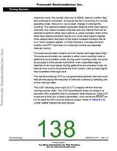
Table 8-1. Timer resolution and capacity
Clock
4.0MHz
1.0MHz
1000ns
1.0µs
8.0MHz 12.0MHz 16.0MHz
4E
E
XTAL
E clock
Period
2.0MHz
500ns
500ns
3.0MHz
333ns
333ns
4.0MHz
250ns
250ns
Control bits
PR[1:0]
1/E
1/E
216/E
– resolution
– overflow
0 0
0 1
1 0
1 1
65.536ms 32.768ms 21.845ms 16.384ms
4.0µs 2.0µs 1.333µs 1.0µs
262.14ms 131.07ms 87.381ms 65.536ms
8.0µs 4.0µs 2.667µs 2.0µs
524.29ms 262.14ms 174.76ms 131.07ms
16.0µs 8.0µs 5.333µs 4.0µs
1049ms 524.29ms 349.53ms 262.14ms
4/E
– resolution
– overflow
218/E
8/E
– resolution
– overflow
219/E
16/E
220/E
– resolution
– overflow
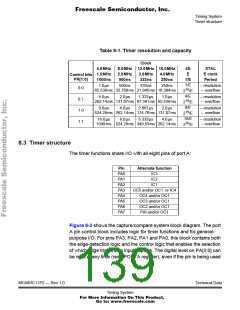
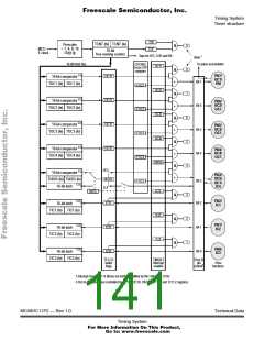
8.3 Timer structure
The timer functions share I/O with all eight pins of port A:
Pin
PA0
PA1
PA2
PA3
PA4
PA5
PA6
PA7
Alternate function
IC3
IC2
IC1
OC5 and/or OC1, or IC4
OC4 and/or OC1
OC3 and/or OC1
OC2 and/or OC1
PAI and/or OC1
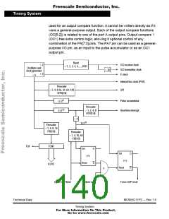
Figure 8-2 shows the capture/compare system block diagram. The port
A pin control block includes logic for timer functions and for general-
purpose I/O. For pins PA3, PA2, PA1 and PA0, this block contains both
the edge-detection logic and the control logic that enables the selection
of which edge triggers an input capture. The digital level on PA[3:0] can
be read at any time (read PORTA register), even if the pin is being used
MC68HC11P2 — Rev 1.0
Technical Data
Timing System
For More Information On This Product,
Go to: www.freescale.com

 FREESCALE [ Freescale ]