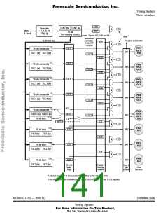
Freescale Semiconductor, Inc.
Timing System
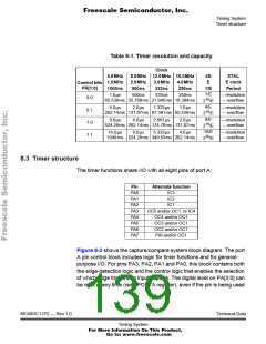
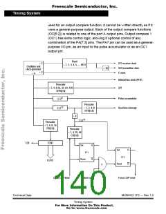
used for an output compare function, it cannot be written directly as if it
were a general-purpose output. Each of the output compare functions
(OC[5:2]) is related to one of the port A output pins. Output compare 1
(OC1) has extra control logic, allowing it optional control of any
combination of the PA[7:3] pins. The PA7 pin can be used as a general-
purpose I/O pin, as an input to the pulse accumulator or as an OC1
output pin.
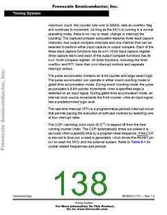
Baud
1, 2, 3, 4, 5,…, 8191
÷
2
2
SCI receiver clock
÷
Oscillator and
SCI transmitter clock
E clock
÷
16
clock generator
÷
÷
4
Internal bus clock (PH2)
SPI
Prescaler
2, 4, 8,16, 32, 64, 128
SPR[2:0]
÷
6
Pulse accumulator
Real time interrupt
E/2
Prescaler
13
÷
1, 2, 4, 8
E/2
RTR[1:0]
÷
4
15
E/2
Prescaler
÷
1, 4, 8, 16
PR[1:0]
Prescaler
÷
1, 4, 16, 64
CR[1:0]
TOF
TCNT
IC/OC
Set
Q
Q
Set
Q
Q
FF1
Reset
FF2
Reset
+
Clear COP timer
System reset
Force COP reset
Technical Data
MC68HC11P2 — Rev 1.0
Timing System
For More Information On This Product,
Go to: www.freescale.com

 FREESCALE [ Freescale ]