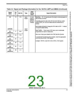
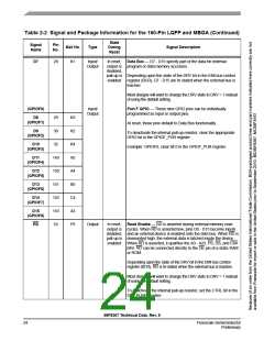
Table 2-2 Signal and Package Information for the 160-Pin LQFP and MBGA (Continued)
State
During
Reset
Signal
Name
Pin
No.
Ball No.
Type
Signal Description
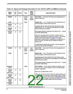
GPIOB0
33
L1
Schmitt
Input/
Output
Input,
pull-up
enabled
Port B GPIO — These four GPIO pins can be programmed as
input or output pins.
(A16)
Output
Address Bus — A16 - A19 specify one of the address lines for
external program or data memory accesses.
GPIOB1
(A17)
34
35
36
L3
L2
Depending upon the state of the DRV bit in the EMI bus control
register (BCR), A16 - A19 and EMI control signals are tri-stated
when the external bus is inactive.
GPIOB2
(A18)
Most designs will want to change the DRV state to DRV = 1 instead
of using the default setting.
GPIOB3
(A19)
M1
After reset, the startup state of GPIOB0 - GPIOB3 (GPIO or
address) is determined as a function of EXTBOOT, EMI_MODE
and the Flash security setting. See Table 4-4 for further
information on when this pin is configured as an address pin at
reset. In all cases, this state may be changed by writing to
GPIOB_PER.
To deactivate the internal pull-up resistor, clear the appropriate
GPIO bit in the GPIOB_PUR register.
GPIOB4
(A20)
37
M2
Schmitt
Input/
Output
Input,
pull-up
enabled
Port B GPIO — These four GPIO pins can be programmed as
input or output pins.
Output
Address Bus — A20 - A23 specify one of the address lines for
external program or data memory accesses.
Depending upon the state of the DRV bit in the EMI bus control
register (BCR), A20–A23 and EMI control signals are tri-stated when
the external bus is inactive.
Most designs will want to change the DRV state to DRV = 1 instead
of using the default setting.
(prescaler_
clock)
Output
Clock Outputs — can be used to monitor the prescaler_clock,
SYS_CLK, SYS_CLK2 or oscillator_clock on GPIOB4 through
GPIOB7, respectively.
GPIOB5
(A21)
(SYS_CLK)
46
47
48
N4
P3
M4
After reset, the default state is GPIO.
These pins can also be used to extend the external address bus
to its full length or to view any of several system clocks. In these
cases, the GPIO_B_PER can be used to individually disable the
GPIO. The CLKOSR register in the SIM (see Part 6.5.7) can then
be used to choose between address and clock functions.
GPIOB6
(A22)
(SYS_CLK2)
GPIOB7
(A23)
(oscillator_
clock)
56F8367 Technical Data, Rev. 9
22
Freescale Semiconductor
Preliminary

 FREESCALE [ Freescale ]