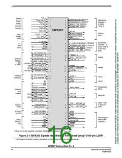
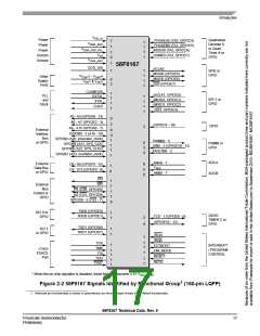
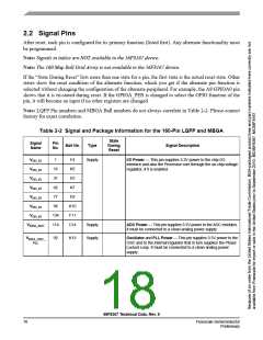
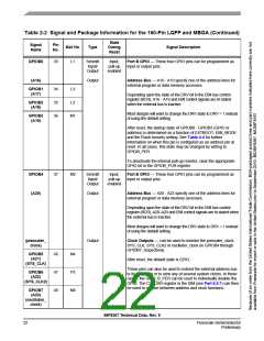
2.2 Signal Pins
After reset, each pin is configured for its primary function (listed first). Any alternate functionality must
be programmed.
Note: Signals in italics are NOT available in the 56F8167 device.
Note: The 160 Map Ball Grid Array is not available in the 56F8167 device.
If the “State During Reset” lists more than one state for a pin, the first state is the actual reset state. Other
states show the reset condition of the alternate function, which you get if the alternate pin function is
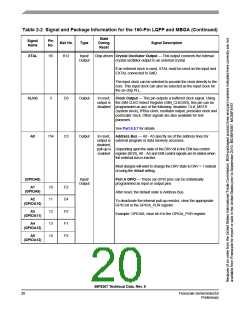
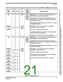
selected without changing the configuration of the alternate peripheral. For example, the A8/GPIOA0 pin
shows that it is tri-stated during reset. If the GPIOA_PER is changed to select the GPIO function of the
pin, it will become an input if no other registers are changed.
Note: LQFP Pin numbers and MBGA Ball numbers do not always correlate in Table 2-2. Please contact
factory for exact correlation.
Table 2-2 Signal and Package Information for the 160-Pin LQFP and MBGA
State
During
Reset
Signal
Name
Pin
No.
Ball No.
Type
Signal Description
VDD_IO
VDD_IO
VDD_IO
VDD_IO
VDD_IO
VDD_IO
VDD_IO
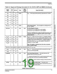
VDDA_ADC
1
F4
K5
Supply
I/O Power — This pin supplies 3.3V power to the chip I/O
interface and also the Processor core through the on-chip voltage
regulator, if it is enabled.
16
31
E5
42
K7
77
E9
96
K10
F11
C14
134
114
Supply
Supply
ADC Power — This pin supplies 3.3V power to the ADC modules.
It must be connected to a clean analog power supply.
VDDA_OSC_
92
K13
Oscillator and PLL Power — This pin supplies 3.3V power to the
OSC and to the internal regulator that in turn supplies the Phase
Locked Loop. It must be connected to a clean analog power
supply.
PLL
56F8367 Technical Data, Rev. 9
18
Freescale Semiconductor
Preliminary

 FREESCALE [ Freescale ]