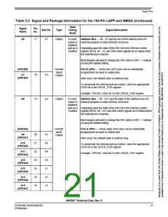
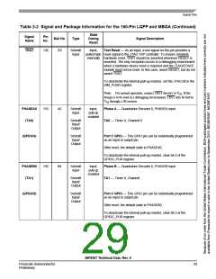
Signal Pins
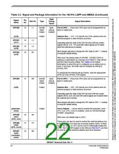
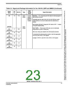
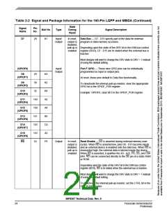
Table 2-2 Signal and Package Information for the 160-Pin LQFP and MBGA (Continued)
State
During
Reset
Signal
Name
Pin
No.
Ball No.
Type
Signal Description
WR
51
L4
Output
In reset, Write Enable — WR is asserted during external memory write
output is cycles. When WR is asserted low, pins D0 - D15 become outputs
disabled, and the device puts data on the bus. When WR is deasserted
pull-up is high, the external data is latched inside the external device. When
enabled
WR is asserted, it qualifies the A0 - A23, PS, DS, and CSn pins.
WR can be connected directly to the WE pin of a static RAM.
Depending upon the state of the DRV bit in the EMI bus control
register (BCR), WR is tri-stated when the external bus is inactive.
Most designs will want to change the DRV state to DRV = 1 instead
of using the default setting.
To deactivate the internal pull-up resistor, set the CTRL bit in the
SIM_PUDR register.
PS
53
N6
Output
In reset, Program Memory Select — This signal is actually CS0 in the
output is EMI, which is programmed at reset for compatibility with the
disabled, 56F80x PS signal. PS is asserted low for external program
pull-up is memory access.
(CS0)
enabled
Depending upon the state of the DRV bit in the EMI bus control
register (BCR), CS0 is tri-stated when the external bus is inactive.
CS0 resets to provide the PS function as defined on the 56F80x
devices.
(GPIOD8)
Input/
Output
Port D GPIO — This GPIO pin can be individually programmed
as an input or output pin.
To deactivate the internal pull-up resistor, clear bit 8 in the
GPIOD_PUR register.
DS
54
L5
Output
In reset, Data Memory Select — This signal is actually CS1 in the EMI,
output is which is programmed at reset for compatibility with the 56F80x
disabled, DS signal. DS is asserted low for external data memory access.
pull-up is
(CS1)
enabled
Depending upon the state of the DRV bit in the EMI bus control
register (BCR), CS1 is tri-stated when the external bus is inactive.
CS1 resets to provide the DS function as defined on the 56F80x
devices.
(GPIOD9)
Input/
Port D GPIO — This GPIO pin can be individually programmed
Output
as an input or output pin.
To deactivate the internal pull-up resistor, clear bit 9 in the
GPIOD_PUR register.
56F8367 Technical Data, Rev. 9
Freescale Semiconductor
Preliminary
25

 FREESCALE [ Freescale ]