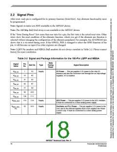
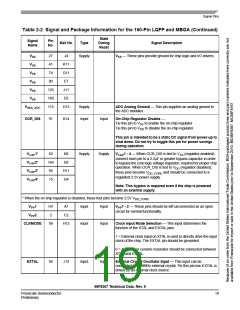
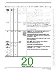
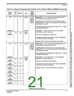
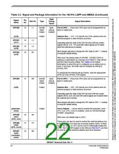
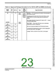
Signal Pins
Table 2-2 Signal and Package Information for the 160-Pin LQFP and MBGA (Continued)
State
During
Reset
Signal
Name
Pin
No.
Ball No.
Type
Signal Description
VSS
VSS
27
41
J4
K11
G11
E7
Supply
VSS — These pins provide ground for chip logic and I/O drivers.
VSS
74
VSS
80
VSS
125
160
115
J11
E6
VSS
VSSA_ADC
D12
Supply
Input
ADC Analog Ground — This pin supplies an analog ground to
the ADC modules.
OCR_DIS
91
K14
Input
On-Chip Regulator Disable —
Tie this pin to VSS to enable the on-chip regulator
Tie this pin to VDD to disable the on-chip regulator
This pin is intended to be a static DC signal from power-up to
shut down. Do not try to toggle this pin for power savings
during operation.
VCAP1*
VCAP2*
VCAP3*
VCAP4*
62
144
95
K8
E8
Supply
Supply
VCAP1 - 4 — When OCR_DIS is tied to VSS (regulator enabled),
connect each pin to a 2.2μF or greater bypass capacitor in order
to bypass the core logic voltage regulator, required for proper chip
operation. When OCR_DIS is tied to VDD (regulator disabled),
H11
G4
these pins become VDD_CORE and should be connected to a
regulated 2.5V power supply.
15
Note: This bypass is required even if the chip is powered
with an external supply.
* When the on-chip regulator is disabled, these four pins become 2.5V VDD_CORE
.
VPP
1
2
141
2
A7
C2
Input
Input
VPP1 - 2 — These pins should be left unconnected as an open
circuit for normal functionality.
VPP
CLKMODE
99
H12
Input
Input
Clock Input Mode Selection — This input determines the
function of the XTAL and EXTAL pins.
1 = External clock input on XTAL is used to directly drive the input
clock of the chip. The EXTAL pin should be grounded.
0 = A crystal or ceramic resonator should be connected between
XTAL and EXTAL.
EXTAL
94
J12
Input
Input
External Crystal Oscillator Input — This input can be
connected to an 8MHz external crystal. Tie this pin low if XTAL is
driven by an external clock source.
56F8367 Technical Data, Rev. 9
Freescale Semiconductor
Preliminary
19

 FREESCALE [ Freescale ]