Register Descriptions
6.3.8.2
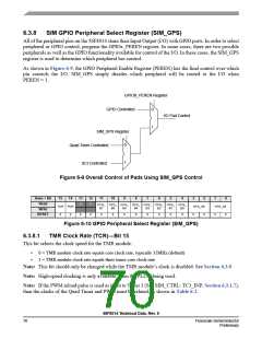
PWM Clock Rate (PCR)—Bit 14
This bit selects the clock speed for the PWM module.
•
•
0 = PWM module clock rate equals core clock rate, typically 32MHz (default)
1 = PWM module clock rate equals three times core clock rate
Note: This bit should only be changed while the PWM module’s clock is disabled. See Section 6.3.9.
Note: High-speed clocking is only available when the PLL is being used.
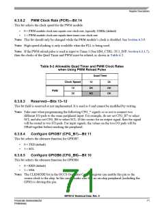
Note: If the PWM reload pulse is used as input to Timer 3 (See SIM_CTRL: TC3_INP, Section 6.3.1.7),
then the clocks of the Quad Timer and PWM must be related, as shown in Table 6-2.
Table 6-2 Allowable Quad Timer and PWM Clock Rates
when Using PWM Reload Pulse
Quad Timer
1X
3X
Clock Speed
1X
3X
OK
NO
OK
OK
PWM
6.3.8.3
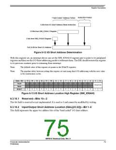
Reserved—Bits 13–12
This bit field is reserved or not implemented. It is read as 0 and cannot be modified by writing.
Note: Take care when programming the following CFG_* signals so as not to connect two
different I/O pads to the same peripheral input. For example, do not set CFG_B7 to select
SCL and also set CFG_B0 to select SCL. If this occurs for an output signal, then the signal
will be routed to two I/O pads. For input signals, the values on the two I/O pads will be
ORed together before reaching the peripheral.
6.3.8.4
Configure GPIOB7 (CFG_B7)—Bit 11
This bit selects the alternate function for GPIOB7.
•
•
0 = TXD (default)
1 = SCL
6.3.8.5
Configure GPIOB6 (CFG_B6)—Bit 10
This bit selects the alternate function for GPIOB6.
•
•
0 = RXD (default)
1 = SDA
Note: The CLKMODE bit in the OCCS Oscillator Control register can enable this pin as the
source clock to the chip. In this mode, make sure that no on-chip peripheral (including the
GPIO) is driving this pin.
56F8014 Technical Data, Rev. 9
Freescale Semiconductor
Preliminary
71

 FREESCALE [ Freescale ]