Register Descriptions
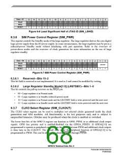
Base + $A
Read
15
14
13
12
11
10
9
8
7
6
5
4
3
2
CLKOSEL
0
1
0
0
0
0
0
0
0
PWM PWM
3
CLK
DIS
PWM1 PWM0
2
Write
0
0
0
0
0
0
0
0
0
0
1
0
0
0
0
RESET
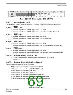
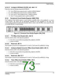
Figure 6-8 CLKO Select Register (SIM_CLKOUT)
6.3.7.1
Reserved—Bits 15–10
This bit field is reserved or not implemented. It is read as 0 and cannot be modified by writing.
6.3.7.2
PWM3—Bit 9
•
•
0 = Peripheral output function of GPIOA[3] is defined to be PWM3
1 = Peripheral output function of GPIOA[3] is defined to be the Relaxation Oscillator Clock
6.3.7.3
PWM2—Bit 8
•
•
0 = Peripheral output function of GPIOA[2] is defined to be PWM2
1 = Peripheral output function of GPIOA[2] is defined to be the system clock
6.3.7.4
PWM1—Bit 7
•
•
0 = Peripheral output function of GPIOA[1] is defined to be PWM1
1 = Peripheral output function of GPIOA[1] is defined to be two times the rate of the system clock
6.3.7.5
PWM0—Bit 6
•
•
0 = Peripheral output function of GPIOA[0] is defined to be PWM0
1 = Peripheral output function of GPIOA[0] is defined to be three times the rate of the system clock
6.3.7.6
Clockout Disable (CLKDIS)—Bit 5
•
•
0 = CLKOUT output is enabled and will output the signal indicated by CLKOSEL
1 = CLKOUT is 0
6.3.7.7
Clockout Select (CLKOSEL)—Bits 4–0
Selects clock to be muxed out on the CLKO pin.
•
•
•
•
•
•
•
00000 = Reserved for factory test—Continuous system clock
01001 = Reserved for factory test—OCCS MSTR OSC clock
01011 = Reserved for factory test—ADC clock
01100 = Reserved for factory test—JTAG TCLK
01101 = Reserved for factory test—Continuous peripheral clock
01110 = Reserved for factory test—Continuous inverted peripheral clock
01111 = Reserved for factory test—Continuous high-speed peripheral clock
56F8014 Technical Data, Rev. 9
Freescale Semiconductor
Preliminary
69

 FREESCALE [ Freescale ]