Register Descriptions
6.3.2.4
External Reset (EXTR)—Bit 3
When set, this bit indicates that the previous system reset was caused by an external reset. It will only be
set if the external reset pin was asserted or remained asserted after the Power-On Reset deasserted.
6.3.2.5
Power-On Reset (POR)—Bit 2
This bit is set during a Power-On Reset.
6.3.2.6
Reserved—Bits 1–0
This bit field is reserved or not implemented. It is read as 0 and cannot be modified by writing.
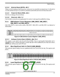
6.3.3
SIM Software Control Registers (SIM_SWC0, SIM_SWC1,
SIM_SWC2, and SIM_SWC3)
Only SIM_SWC0 is shown in this section. SIM_SWC1, SIM_SWC2, and SIM_SWC3 are identical in
functionality.
Base + $2
Read
15
14
13
12
11
10
9
8
7
6
5
4
3
2
1
0
Software Control Data 0
Write
0
0
0
0
0
0
0
0
0
0
0
0
0
0
0
0
RESET
Figure 6-4 SIM Software Control Register 0 (SIM_SWC0)
Software Control Data 0 (FIELD)—Bits 15–0
6.3.3.1
This register is reset only by the Power-On Reset (POR). It has no part-specific functionality and is
intended for use by a software developer to contain data that will be unaffected by the other reset sources
(RESET pin, software reset, and COP reset).
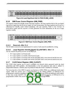
6.3.4
Most Significant Half of JTAG ID (SIM_MSHID)
This read-only register displays the most significant half of the JTAG ID for the chip. This register reads
$01F2.
Base + $6
Read
15
14
13
12
11
10
9
8
7
6
5
4
3
2
1
0
0
0
0
0
0
0
0
1
1
1
1
1
0
0
1
0
Write
RESET
0
0
0
0
0
0
0
1
1
1
1
1
0
0
1
0
Figure 6-5 Most Significant Half of JTAG ID (SIM_MSHID)
6.3.5
Least Significant Half of JTAG ID (SIM_LSHID)
This read-only register displays the least significant half of the JTAG ID for the chip. This register reads
$401D.
56F8014 Technical Data, Rev. 9
Freescale Semiconductor
Preliminary
67

 FREESCALE [ Freescale ]