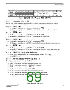
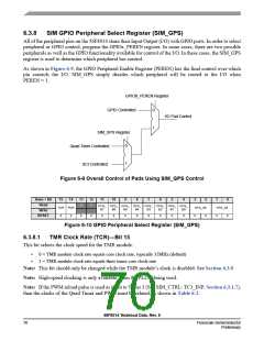
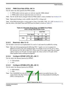
Register Descriptions
6.3.8.13 Configure GPIOA4[1:0] (CFG_A4)—Bits 1–0
These bits select the alternate function for GPIOA4.
•
•
•
•
00 = Select PWM4 when peripheral mode is enabled in GPIOA4 (default)
01 = Select PWM4 when peripheral mode is enabled in GPIOA4
10 = Select FAULT1 when peripheral mode is enabled in GPIOA4
11 = Select T2 when peripheral mode is enabled in GPIOA4
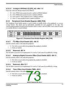
6.3.9
Peripheral Clock Enable Register (SIM_PCE)
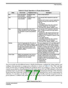
The Peripheral Clock Enable register is used to enable or disable clocks to the peripherals as a power
savings feature. The clocks can be individually controlled for each peripheral on the chip. The
corresponding peripheral should itself be disabled while its clock is shut off. IPBus writes cannot be made
to a module that has its clock disabled.
Base + $C
Read
15
14
13
12
11
10
9
8
7
6
5
4
3
2
1
0
0
0
0
0
0
0
0
0
0
0
I2C
ADC
TMR
SCI
SPI
PWM
Write
0
0
0
0
0
0
0
0
0
0
0
0
0
0
0
0
RESET
Figure 6-11 Peripheral Clock Enable Register (SIM_PCE)
2
6.3.9.1
I C IPBus Clock Enable (I2C)—Bit 15
Each bit controls clocks to the indicated peripheral.
•
•
0 = The clock is not provided to the peripheral (the peripheral is disabled)
1 = Clocks are enabled
6.3.9.2
Reserved—Bit 14
This bit field is reserved or not implemented. It is read as 0 and cannot be modified by writing.
6.3.9.3
Analog-to-Digital Converter IPBus Clock Enable (ADC)—Bit 13
Each bit controls clocks to the indicated peripheral.
•
•
0 = The clock is not provided to the peripheral (the peripheral is disabled)
1 = Clocks are enabled
6.3.9.4
Reserved—Bits 12–7
This bit field is reserved or not implemented. It is read as 0 and cannot be modified by writing.
6.3.9.5
Timer IPBus Clock Enable (TMR)—Bit 6
Each bit controls clocks to the indicated peripheral.
•
•
0 = The clock is not provided to the peripheral (the peripheral is disabled)
1 = Clocks are enabled
56F8014 Technical Data, Rev. 9
Freescale Semiconductor
Preliminary
73

 FREESCALE [ Freescale ]