6.3.9.6
Reserved—Bit 5
This bit field is reserved or not implemented. It is read as 0 and cannot be modified by writing.
6.3.9.7
SCI IPBus Clock Enable (SCI)—Bit 4
Each bit controls clocks to the indicated peripheral.
•
•
0 = The clock is not provided to the peripheral (the peripheral is disabled)
1 = Clocks are enabled
6.3.9.8
Reserved—Bit 3
This bit field is reserved or not implemented. It is read as 0 and cannot be modified by writing.
6.3.9.9
SPI IPBus Clock Enable (SPI)—Bit 2
Each bit controls clocks to the indicated peripheral.
•
•
0 = The clock is not provided to the peripheral (the peripheral is disabled)
1 = Clocks are enabled
6.3.9.10 Reserved—Bit 1
This bit field is reserved or not implemented. It is read as 0 and cannot be modified by writing.
6.3.9.11 PWM IPBus Clock Enable (PWM)—Bit 0
Each bit controls clocks to the indicated peripheral.
•
•
0 = The clock is not provided to the peripheral (the peripheral is disabled)
1 = Clocks are enabled
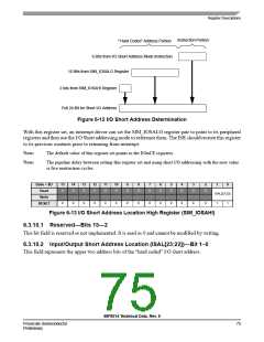
6.3.10 I/O Short Address Location Register (SIM_IOSAHI and
SIM_IOSALO)
The I/O Short Address Location registers are used to specify the memory referenced via the I/O short
address mode. The I/O short address mode allows the instruction to specify the lower six bits of address;
the upper address bits are not directly controllable. This register set allows limited control of the full
address, as shown in Figure 6-12.
56F8014 Technical Data, Rev. 9
74
Freescale Semiconductor
Preliminary

 FREESCALE [ Freescale ]