Base + $7
Read
15
14
13
12
11
10
9
8
7
6
5
4
3
2
1
0
0
1
0
0
0
0
0
0
0
0
0
1
1
1
0
1
Write
0
1
0
0
0
0
0
0
0
0
0
1
1
1
0
1
RESET
Figure 6-6 Least Significant Half of JTAG ID (SIM_LSHID)
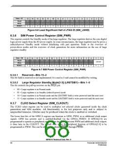
6.3.6
SIM Power Control Register (SIM_PWR)
This register controls the Standby mode of the large regulator. The large regulator derives the core digital
logic power supply from the IO power supply. In some circumstances, the large regulator may be put in a
reduced-power Standby mode without interfering with part operation. Refer to the overview of
power-down modes and the overview of clock generation for more information on the use of large
regulator standby.
Base + $8
Read
15
14
13
12
11
10
9
8
7
6
5
4
3
2
1
0
0
0
0
0
0
0
0
0
0
0
0
0
0
0
LRSTDBY
Write
0
0
0
0
0
0
0
0
0
0
0
0
0
0
0
0
RESET
Figure 6-7 SIM Power Control Register (SIM_PWR)
6.3.6.1
Reserved—Bits 15–2
This bit field is reserved or not implemented. It is read as 0 and cannot be modified by writing.
6.3.6.2
Large Regulator Standby Mode[1:0] (LRSTDBY)—Bits 1–0
This bit controls the pull-up resistors on the IRQA pin.
•
•
•
•
00 = Large regulator is in Normal mode
01 = Large regulator is in Standby (reduced-power) mode
10 = Large regulator is in Normal mode and the LRSTDBY field is write-protected until the next reset
11 = Large regulator is in Standby mode and the LRSTDBY field is write-protected until the next reset
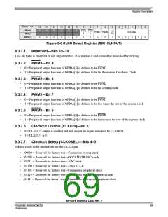
6.3.7
CLKO Select Register (SIM_CLKOUT)
The CLKO select register can be used to multiplex out selected clocks generated inside the clock
generation and SIM modules. All functionality is for test purposes only and is subject to
unspecified latencies. Glitches may be produced when the clock is enabled or switched.
The lower four bits of the GPIO A register can function as GPIO, PWM, or as additional clock output
signals. GPIO has priority and is enabled/disabled via the GPIOA_PEREN. If GPIOA[3:0] are
programmed to operate as peripheral outputs, then the choice between PWM and additional clock outputs
is done here in the CLKOUT. The default state is for the peripheral function of GPIOA[3:0] to be
programmed as PWM. This can be changed by altering PWM3 through PWM0.
56F8014 Technical Data, Rev. 9
68
Freescale Semiconductor
Preliminary

 FREESCALE [ Freescale ]