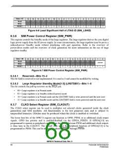
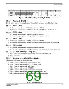
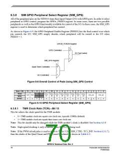
6.3.8.6
Configure GPIOB5 (CFG_B5)—Bit 9
This bit selects the alternate function for GPIOB5.
•
•
0 = T1 (default)
1 = FAULT3
6.3.8.7
Configure GPIOB4 (CFG_B4)—Bit 8
This bit selects the alternate function for GPIOB4.
•
•
0 = T0 (default)
1 = CLKO
6.3.8.8
Configure GPIOB3 (CFG_B3)—Bit 7
This bit selects the alternate function for GPIOB3.
•
•
0 = MOSI (default)
1 = T3
6.3.8.9
Configure GPIOB2 (CFG_B2)—Bit 6
This bit selects the alternate function for GPIOB2.
•
•
0 = MISO (default)
1 = T2
6.3.8.10 Configure GPIOB1 (CFG_B1)—Bit 5
This bit selects the alternate function for GPIOB1.
•
•
0 = SS (default)
1 = SDA
6.3.8.11 Configure GPIOB0 (CFG_B0)—Bit 4
This bit selects the alternate function for GPIOB0.
•
•
0 = SCLK (default)
1 = SCL
6.3.8.12 Configure GPIOA5[1:0] (CFG_A5)—Bits 3–2
These bits select the alternate function for GPIOA5.
•
•
•
•
00 = Select PWM5 when peripheral mode is enabled in GPIOA5 (default)
01 = Select PWM5 when peripheral mode is enabled in GPIOA5
10 = Select FAULT2 when peripheral mode is enabled in GPIOA5
11 = Select T3 when peripheral mode is enabled in GPIOA5
56F8014 Technical Data, Rev. 9
72
Freescale Semiconductor
Preliminary

 FREESCALE [ Freescale ]