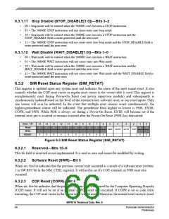
6.3.8
SIM GPIO Peripheral Select Register (SIM_GPS)
All of the peripheral pins on the 56F8014 share their Input/Output (I/O) with GPIO ports. In order to select
peripheral or GPIO control, program the GPIOx_PEREN register. In some cases, there are two possible
peripherals as well as the GPIO functionality available for control of the I/O. In these cases, the SIM_GPS
register is used to determine which peripheral has control.
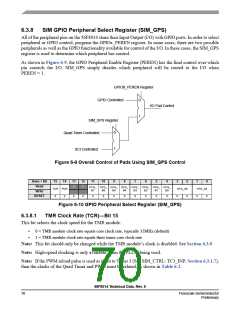
As shown in Figure 6-9, the GPIO Peripheral Enable Register (PEREN) has the final control over which
pin controls the I/O. SIM_GPS simply decides which peripheral will be routed to the I/O when
PEREN = 1.
GPIOB_PEREN Register
GPIO Controlled
0
1
I/O Pad Control
SIM_GPS Register
0
1
Quad Timer Controlled
SCI Controlled
Figure 6-9 Overall Control of Pads Using SIM_GPS Control
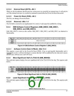
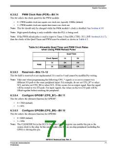
Base + $B
Read
15
14
13
12
11
10
9
8
7
6
5
4
3
2
1
0
0
0
CFG_ CFG_ CFG_ CFG_ CFG_ CFG_ CFG_ CFG_
B7
TCR PCR
CFG_A5
CFG_A4
B6
B5
B4
B3
B2
B1
B0
Write
0
0
0
0
0
0
0
0
0
0
0
0
0
0
0
0
RESET
Figure 6-10 GPIO Peripheral Select Register (SIM_GPS)
6.3.8.1
TMR Clock Rate (TCR)—Bit 15
This bit selects the clock speed for the TMR module.
•
•
0 = TMR module clock rate equals core clock rate, typically 32MHz (default)
1 = TMR module clock rate equals three times core clock rate
Note: This bit should only be changed while the TMR module’s clock is disabled. See Section 6.3.9.
Note: High-speed clocking is only available when the PLL is being used.
Note: If the PWM reload pulse is used as input to Timer 3 (See SIM_CTRL: TC3_INP, Section 6.3.1.7),
then the clocks of the Quad Timer and PWM must be related, as shown in Table 6-2.
56F8014 Technical Data, Rev. 9
70
Freescale Semiconductor
Preliminary

 FREESCALE [ Freescale ]