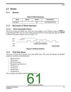
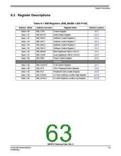
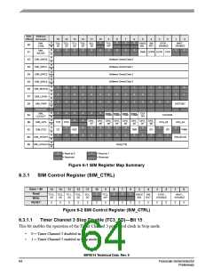
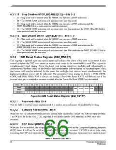
Register Descriptions
6.3.1.2
Timer Channel 2 Stop Disable (TC2_SD)—Bit 14
This bit enables the operation of the Timer Channel 2 peripheral clock in Stop mode.
•
•
0 = Timer Channel 2 disabled in Stop mode
1 = Timer Channel 2 enabled in Stop mode
6.3.1.3
Timer Channel 1 Stop Disable (TC1_SD)—Bit 13
This bit enables the operation of the Timer Channel 1 peripheral clock in Stop mode.
•
•
0 = Timer Channel 1 disabled in Stop mode
1 = Timer Channel 1 enabled in Stop mode
6.3.1.4
Timer Channel 0 Stop Disable (TC0_SD)—Bit 12
This bit enables the operation of the Timer Channel 0 peripheral clock in Stop mode.
•
•
0 = Timer Channel 0 disabled in Stop mode
1 = Timer Channel 0 enabled in Stop mode
6.3.1.5
SCI Stop Disable (SCI_SD)—Bit 11
This bit enables the operation of the SCI peripheral clock in Stop mode. This is recommended for use in
LIN mode so that the SCI can generate interrupts and recover from Stop mode while the LIN interface is
in Sleep mode and using Stop mode to reduce power consumption.
•
•
0 = SCI disabled in Stop mode
1 = SCI enabled in Stop mode
6.3.1.6
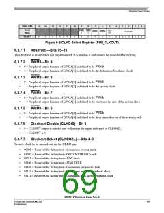
Reserved—Bit 10
This bit field is reserved or not implemented. It is read as 0 and cannot be modified by writing.
6.3.1.7
Timer Channel 3 Input (TC3_INP)—Bit 9
This bit selects the input of Timer Channel 3 to be from the PWM or GPIO.
•
•
1 = Timer Channel 3 Input from PWM reload_sync signal
0 = Timer Channel 3 Input controlled by SIM_GPS register CFG_B3 and CFG_A5 fields
6.3.1.8
Reserved—Bits 8–6
This bit field is reserved or not implemented. It is read as 0 and cannot be modified by writing.
6.3.1.9
OnCE Enable (ONCEEBL)—Bit 5
•
•
0 = OnCE clock to 56800E core enabled when core TAP is enabled
1 = OnCE clock to 56800E core is always enabled
6.3.1.10 Software Reset (SWRST)—Bit 4
Writing 1 to this field will cause the part to reset.
56F8014 Technical Data, Rev. 9
Freescale Semiconductor
Preliminary
65

 FREESCALE [ Freescale ]