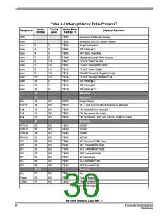
1
Table 4-2 Interrupt Vector Table Contents
Vector
Number
Priority
Level
Vector Base
Address +
Peripheral
Interrupt Function
Reserved for Reset Overlay2
core
P:$00
core
core
core
core
core
core
core
core
core
core
core
core
core
P:$02
P:$04
P:$06
P:$08
P:$0A
P:$0C
P:$0E
P:$10
P:$12
P:$14
P:$16
P:$18
P:$1A
Reserved for COP Reset Overlay
Illegal Instruction
2
3
4
5
6
7
8
9
3
3
3
3
SW Interrupt 3
HW Stack Overflow
Misaligned Long Word Access
EOnCE Step Counter
EOnCE Breakpoint Unit 0
EOnCE Trace Buffer
EOnCE Transmit Register Empty
EOnCE Receive Register Full
SW Interrupt 2
1-3
1-3
1-3
1-3
1-3
2
10
11
12
13
14
15
16
17
18
19
20
21
22
23
24
25
26
27
28
29
30
31
32
33, 34
35
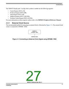
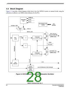
1
SW Interrupt 1
0
SW Interrupt 0
Reserved
Reserved
PS
0-2
0-2
0-2
0-2
0-2
P:$20
P:$22
P:$24
P:$26
P:$28
Power Sense
OCCS
FM
PLL Lock, Loss of Clock Reference Interrupt
FM Access Error Interrupt
FM Command Complete
FM Command, data and address Buffers Empty
Reserved
FM
FM
GPIOD
GPIOC
GPIOB
GPIOA
SPI
0-2
0-2
0-2
0-2
0-2
0-2
0-2
0-2
0-2
0-2
0-2
P:$2C
P:$2E
P:$30
P:$32
P:$34
P:$36
P:$38
P:$3A
P:$3C
P:$3E
P:$40
GPIOD
GPIOC
GPIOB
GPIOA
SPI Receiver Full / Error
SPI Transmitter Empty
SCI Transmitter Empty
SCI Transmitter Idle
SCI Reserved
SPI
SCI
SCI
SCI
SCI
SCI Receiver Error
SCI Receiver Full
SCI
Reserved
I2C
I2C
0-2
P:$46
Timer
Timer
36
37
0-2
0-2
P:$48
P:$4A
Timer Channel 0
Timer Channel 1
(Continues next page)
56F8014 Technical Data, Rev. 9
30
Freescale Semiconductor
Preliminary

 FREESCALE [ Freescale ]