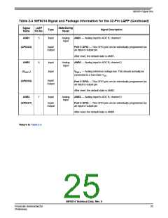
Pin Descriptions
3.5 Pin Descriptions
3.5.1
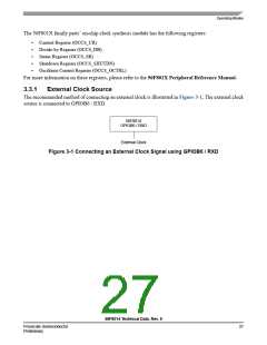
External Reference (GPIOB6 / RXD)
The relaxation oscillator is included on chip and the reset mode is to use this as the clock source for the
chip. The user then has the option of switching to an external clock reference if desired.
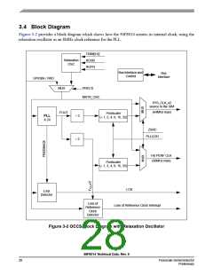
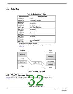
Part 4 Memory Map
4.1 Introduction
The 56F8014 device is a 16-bit motor-control chip based on the 56800E core. It uses a Harvard-style
architecture with two independent memory spaces for Data and Program. On-chip RAM is used in both
spaces and Flash memory is used only in Program space.
This section provides memory maps for:
•
•
Program Address Space, including the Interrupt Vector Table
Data Address Space, including the EOnCE Memory and Peripheral Memory Maps
On-chip memory sizes for the device are summarized in Table 4-1. Flash memories’ restrictions are
identified in the “Use Restrictions” column of Table 4-1.
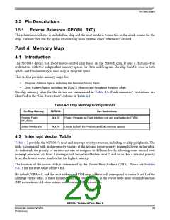
Table 4-1 Chip Memory Configurations
On-Chip Memory
56F8014
Use Restrictions
Program Flash
(PFLASH)
8k x 16
Erase / Program via Flash interface unit and word writes to CDBW
Unified RAM (ram)
2k x 16
Usable by both the Program and Data memory spaces
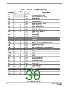
4.2 Interrupt Vector Table
Table 4-2 provides the 56F8014’s reset and interrupt priority structure, including on-chip peripherals. The
table is organized with higher-priority vectors at the top and lower-priority interrupts lower in the table.
As indicated, the priority of an interrupt can be assigned to different levels, allowing some control over
interrupt priorities. All level 3 interrupts will be serviced before level 2, and so on. For a selected priority
level, the lowest vector number has the highest priority.
The location of the vector table is determined by the Vector Base Address (VBA). Please see Section
5.6.11 for the reset value of the VBA.
By default, VBA = 0, and the reset address and COP reset address will correspond to vector 0 and 1 of the
interrupt vector table. In these instances, the first two locations in the vector table must contain branch or
JMP instructions. All other entries must contain JSR instructions.
56F8014 Technical Data, Rev. 9
Freescale Semiconductor
Preliminary
29

 FREESCALE [ Freescale ]