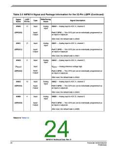
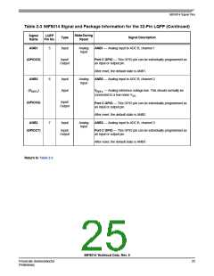
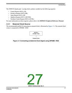
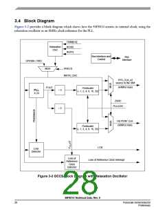
3.4 Block Diagram
Figure 3-2 provides a block diagram which shows how the 56F8014 creates its internal clock, using the
relaxation oscillator as an 8MHz clock reference for the PLL.
TRIM[9:0]
Relaxation
OSC
ROSB
ROPD
Bus Interface and
Control
Bus
Interface
GPIOB6 / RXD
MUX
PRECS
MSTR_OSC
SYS_CLK_x2
source to the SIM
(64MHz max)
FOUT
Postscaler
÷ 3
÷ 2
PLL
X 24
(÷ 1, 2, 4, 8, 16, 32)
ZSRC
PLLCOD
HS PERF CLK
(96MHz max)
Postscaler
(÷ 1, 2, 4, 8, 16, 32)
LCK
Lock
Detector
Loss of
Reference
Clock
Loss of Reference Clock Interrupt
Detector
Figure 3-2 OCCS Block Diagram with Relaxation Oscillator
56F8014 Technical Data, Rev. 9
28
Freescale Semiconductor
Preliminary

 FREESCALE [ Freescale ]