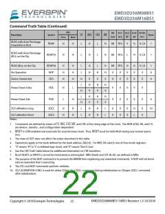
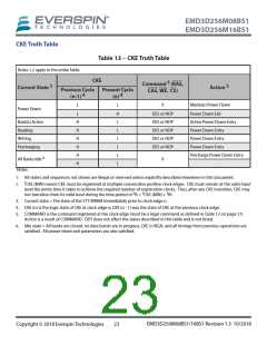
EMD3D256M08BS1
EMD3D256M16BS1
t
t
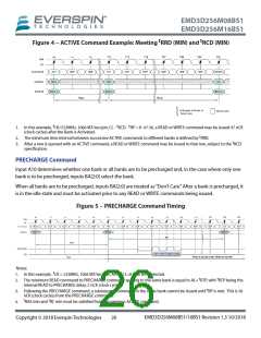
Figure 4 – ACTIVE Command Example: Meeting RRD (MIN) and RCD (MIN)
T12
T13
T14
TT6467
T6478
T49
T68
T50
69
f
t
t
1. In this example, CK=533MHz, 1066 MT/sec/pin, CL - RCD - RP = 8- 47-36, a READ or WRITE command may be issued 47 nCK
(clock cycles) after the Bank is Activated.
t
2. The minimum time interval between successive ACTIVE commands to different banks is defined by RRD.
3. After a row is opened with an ACTIVE command, a READ or WRITE command may be issued to that row, subject to the RCD
t
specification.
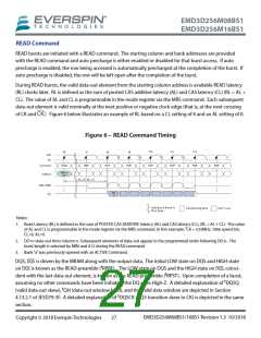
PRECHARGE Command
Input A10 determines whether one bank or all banks are to be precharged and, in the case where only one
bank is to be precharged, inputs BA[2:0] select the bank.
When all banks are to be precharged, inputs BA[2:0] are treated as “Don’t Care.”After a bank is precharged, it
is in the idle state and must be activated prior to any READ or WRITE commands being issued.
Figure 5 – PRECHARGE Command Timing
T31
T19
T32
T20
T33
T21
t
t
PRCD (to next RD or WR), RPRAS (to next PRE)
Notes:
1. In this example, CK = 533MHz, 1066 MT/sec/pin, AL=0, CL=8 with BC4 selected.
2. The minimum READ command to PRECHARGE command spacing to the same bank is equal to AL+ RTP, with RTP being the
internal READ to PRECHARGE delay, 5 nCK (clock cycles).
f
t
t
t
3. Following the PRECHARGE command, a subsequent command to the same bank cannot be issued until RP is met. This is 36
nCK (clock cycles) from the PRECHARGE command.
t
t
4.
RAS min and RC min must be satisfied from the previous ACTIVE command.
EMD3D256M08BS1/16BS1 Revision 1.3 10/2018
Copyright © 2018 Everspin Technologies
26

 EVERSPIN [ Everspin Technologies ]