EMD3D256M08BS1
EMD3D256M16BS1
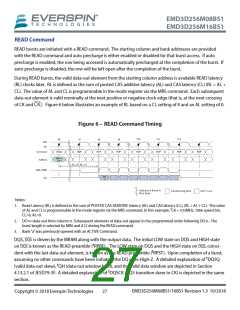
and any additional input data will be ignored.
Data for any WRITE burst may be concatenated with a subsequent WRITE command to provide a continuous
t
flow of input data. The new WRITE command can be CCD clocks following the previous WRITE command.
The first data element from the new burst is applied after the last element of a completed burst. Standard
JESD79-3F Figure 51, WRITE(BL8) to WRITE(BL8) and Figure 52, WRITE (BC4) to WRITE (BC4) OTF illustrate con-
catenated bursts.
t
Data for any WRITE burst may be followed by a subsequent READ command after WTR has been met (see
Standard JESD79-3F Figure 53, WRITE (BL8) to READ (BC4/BL8) OTF. ) Additional WRITE burst diagrams are
given in Section 4.14, WRITE Operation.
t
Data for any WRITE burst may be followed by a subsequent PRECHARGE command, providing WR has
been met, as shown in Standard JESD79-3F Figures 49 and 50. Please note that in Write followed by a PRE-
t
CHARGE, the MRAM RP needs to be observed for a given CL.
t
t
Both WTR and WR starting time may vary, depending on the mode register settings (fixed BC4, BL8 versus
OTF).
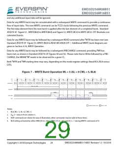
Figure 7 – WRITE Burst Operation WL = 5 (AL = 0 CWL = 5, BL8)
Notes:
1. BL8, WL= 5; AL=0, CWL=5
2. DIN n = data-in from column n.
3. NOP commands are shown for ease of illustration; other commands may be valid at these times.
4. BL8 setting activated by either MR0 [A1:0= 00] or MR0 [ A1:0 = 01] and A12 = 1 during WRITE command at T0
EMD3D256M08BS1/16BS1 Revision 1.3 10/2018
Copyright © 2018 Everspin Technologies
29

 EVERSPIN [ Everspin Technologies ]