EMD3D256M08BS1
EMD3D256M16BS1
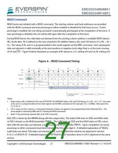
Data from any READ burst may be concatenated with data from a subsequent READ command to provide a
continuous flow of data. The first data element from the new burst follows the last element of a completed
t
burst. The new READ command should be issued CCD cycles after the first READ command. This is shown
t
for BL8 in Standard JESD79-3F Figure 33. If BC4 is enabled, CCD must still be met, which will cause a gap in
the data output, as shown in JESD79-3F Figure 34. The DDR3 MRAM does not allow interrupting or truncat-
ing any READ burst. Data from any READ burst must be completed before a subsequent WRITE burst is al-
lowed. An example of a READ burst followed by a WRITE burst for BL8 can be found in JESD79-3F Figure 35,
READ (BL8) to WRITE (BL8). READ to WRITE timing for BC4 can be found in JESD79-3F Figure 36, READ (BC4) to
WRITE (BC4) OTF. To ensure the READ data is completed before the WRITE data is on the bus, the minimum
t
t
READ-to-WRITE timing is RL + CCD - WL + 2 CK.
For additional information on the READ command, please refer to JESD79-3F Section 4.13. Please note that
t
in READ followed by a PRECHARGE, the MRAM RP needs to be observed for a given CL.
WRITE Command
WRITE bursts are initiated with a WRITE command. The starting column and bank addresses are provided
with the WRITE command, and auto precharge is either enabled or disabled for that access. If auto-pre-
charge is selected, the row being accessed is precharged at the end of the WRITE burst. If auto-precharge is
not selected, the row will remain open for subsequent accesses. After a WRITE command has been issued,
the WRITE burst may not be interrupted.
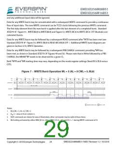
During WRITE bursts, the first valid data-in element is registered on the first rising edge of DQS immediately
following the WRITE latency (WL) clock time. Data elements will continue to be registered on successive
edges of DQS.
WRITE latency (WL) is defined as the sum of posted CAS additive latency (AL) and CAS WRITE latency (CWL):
WL = AL + CWL. The values of AL and CWL are programmed in the MR0 and MR2 registers respectively.
Only AL=0 is supported. Prior to the first valid DQS edge, a full cycle is needed (including a dummy cross-
over of DQS, DQS) and specified as the WRITE preamble shown in “Figure 7 – WRITE Burst Operation WL =
5 (AL = 0 CWL = 5, BL8)”on page 29. The half cycle on DQS following the last data-in element is known as
the WRITE postamble.
t
The time between the WRITE command and the first valid edge of DQS is WL clocks DQSS. Standard
t
t
t
JESD79-3F Figure 43 includes DQSS (MIN), DQSS (NOM) and DQSS (MAX) cases.
Data may be masked from completing a WRITE using data mask. The data mask occurs on the DM ball
aligned to the WRITE data. If DM is LOW, the WRITE completes normally. If DM is HIGH, that bit of data is
masked.
Upon completion of a burst, assuming no other commands have been initiated, the DQ will remain High-Z,
EMD3D256M08BS1/16BS1 Revision 1.3 10/2018
Copyright © 2018 Everspin Technologies
28

 EVERSPIN [ Everspin Technologies ]