EMD3D256M08BS1
EMD3D256M16BS1
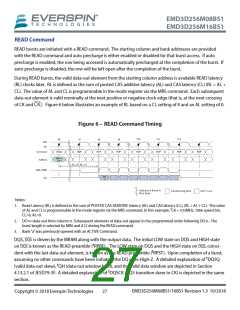
READ Command
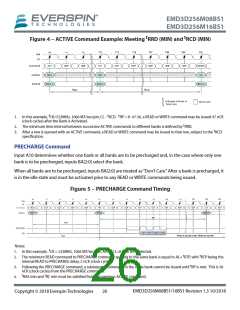
READ bursts are initiated with a READ command. The starting column and bank addresses are provided
with the READ command and auto precharge is either enabled or disabled for that burst access. If auto
precharge is enabled, the row being accessed is automatically precharged at the completion of the burst. If
auto precharge is disabled, the row will be left open after the completion of the burst.
During READ bursts, the valid data-out element from the starting column address is available READ latency
(RL) clocks later. RL is defined as the sum of posted CAS additive latency (AL) and CAS latency (CL) (RL = AL +
CL). The value of AL and CL is programmable in the mode register via the MRS command. Each subsequent
data-out element is valid nominally at the next positive or negative clock edge (that is, at the next crossing
of CK and CK.) Figure 6 below illustrates an example of RL based on a CL setting of 8 and an AL setting of 0.
Figure 6 – READ Command Timing
T10
T11
T12
Tꢀ
T8
Tꢁ
Notes:
1. Read Latency (RL) is defined as the sum of POSTED CAS ADDITIVE latency (AL) and CAS latency (CL), (RL = AL + CL). -The value
f
of AL and CL is programmable in the mode register via the MRS command. In this example, CK = 533MHz, 1066 speed bin,
CL=8, AL=0.
2. DO n=data-out from column n. Subsequent elements of data-out appear in the programmed order following DO n. -The
burst length is selected by MR0 and A12 during the READ command.
3. Bank “a”was previously opened with an ACTIVE Command.
DQS, DQS is driven by the MRAM along with the output data. The initial LOW state on DQS and HIGH state
t
on DQS is known as the READ preamble ( RPRE). The LOW state on DQS and the HIGH state on DQS, coinci-
t
dent with the last data-out element, is known as the READ postamble ( RPST). Upon completion of a burst,
t
assuming no other commands have been initiated, the DQ goes High-Z. A detailed explanation of DQSQ
t
(valid data-out skew), QH (data-out window hold), and the valid data window are depicted in Section
t
4.13.2.1 of JESD79-3F. A detailed explanation of DQSCK (DQS transition skew to CK) is depicted in the same
section.
EMD3D256M08BS1/16BS1 Revision 1.3 10/2018
Copyright © 2018 Everspin Technologies
27

 EVERSPIN [ Everspin Technologies ]