EMD3D256M08BS1
EMD3D256M16BS1
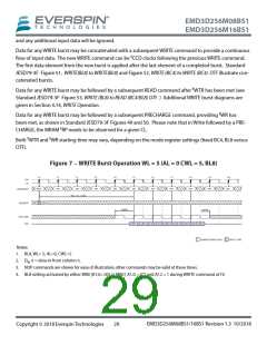
COMMAND DESCRIPTIONS
The 256Mb STT-MRAM is fully compatible with the command descriptions of JESD79-3F, section 4, with the
following additional considerations:
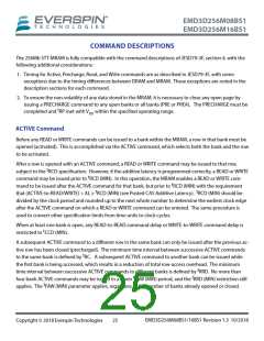
1. Timing for Active, Precharge, Read, and Write commands are as described in JESD79-3F, with some
exceptions due to the timing differences between DRAM and MRAM. These exceptions are noted in the
description sections for each command.
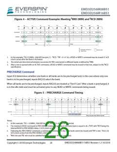
2. To ensure the non-volatility of any data stored in the MRAM, it is necessary to close any open page by
issuing a PRECHARGE command to any open banks or all banks (PRE or PREA). The PRECHARGE must be
t
completed and RP met with VDD within the specified operating range.
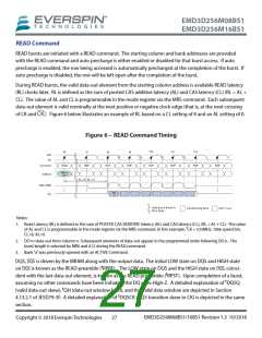
ACTIVE Command
Before any READ or WRITE commands can be issued to a bank within the MRAM, a row in that bank must be
opened (activated). This is accomplished via the ACTIVE command, which selects both the bank and the row
to be activated.
After a row is opened with an ACTIVE command, a READ or WRITE command may be issued to that row,
t
subject to the RCD specification. However, if the additive latency is programmed correctly, a READ or WRITE
t
command may be issued prior to RCD (MIN). In this operation, the MRAM enables a READ or WRITE com-
t
mand to be issued after the ACTIVE command for that bank, but prior to RCD (MIN) with the requirement
t
t
that (ACTIVE-to-READ/WRITE) + AL ≥ RCD (MIN) (see Posted CAS Additive Latency). RCD (MIN) should be
divided by the clock period and rounded up to the next whole number to determine the earliest clock edge
after the ACTIVE command on which a READ or WRITE command can be entered. The same procedure is
used to convert other specification limits from time units to clock cycles.
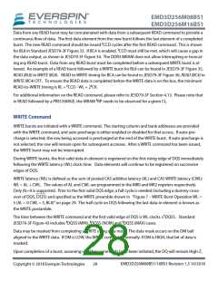
When at least one bank is open, any READ-to-READ command delay or WRITE-to-WRITE command delay is
t
restricted to CCD (MIN).
A subsequent ACTIVE command to a different row in the same bank can only be issued after the previous ac-
tive row has been closed (precharged). The minimum time interval between successive ACTIVE commands
t
to the same bank is defined by RC. A subsequent ACTIVE command to another bank can be issued while
the first bank is being accessed, which results in a reduction of total row-access overhead. The minimum
t
time interval between successive ACTIVE commands to different banks is defined by RRD. No more than
t
t
four bank ACTIVE commands may be issued in a given FAW (MIN) period, and the RRD (MIN) restriction still
t
applies. The FAW (MIN) parameter applies, regardless of the number of banks already opened or closed.
EMD3D256M08BS1/16BS1 Revision 1.3 10/2018
Copyright © 2018 Everspin Technologies
25

 EVERSPIN [ Everspin Technologies ]