EMD3D256M08BS1
EMD3D256M16BS1
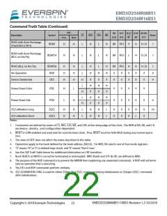
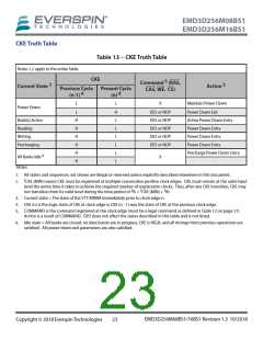
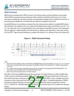
CKE Truth Table
Table 13 – CKE Truth Table
Notes 1,2 apply to the entire Table.
CKE
Previous Cycle
5
Command (RAS,
3
5
Current State
Action
Present Cycle
CAS, WE. CS)
4
4
(n-1)
(n)
L
L
H
L
L
L
L
L
L
X
Maintain Power Down
Power Down Exit
Power Down
L
DES or NOP
DES or NOP
DES or NOP
DES or NOP
DES or NOP
Bank(s) Active
Reading
H
H
H
H
H
H
Active Power Down Entry
Power Down Entry
Power Down Entry
Power Down Entry
Precharge Power Down Entry
-
Writing
Precharging
6
All Banks Idle
Notes:
X
1. All states and sequences not shown are illegal or reserved unless explicitly described elsewhere in this document.
t
2.
CKE (MIN) means CKE must be registered at multiple consecutive positive clock edges. CKE must remain at the valid input
level the entire time it takes to achieve the required number of registration clocks. Thus, after any CKE transition, CKE may
not transition from its valid level during the time period of IS + CKE (MIN) + IH.
t
t
t
3. Current state = The state of the STT-MRAM immediately prior to clock edge n.
4. CKE (n) is the logic state of CKE at clock edge n; CKE (n - 1) was the state of CKE at the previous clock edge.
5. COMMAND is the command registered at the clock edge (must be a legal command as defined in Table 12 on page 21)
Action is a result of COMMAND. ODT does not affect the states described in this table and is not listed.
6. Idle state = All banks are closed, no data bursts are in progress, CKE is HIGH, and all timings from previous operations are
satisfied. All power-down exit parameters are also satisfied.
EMD3D256M08BS1/16BS1 Revision 1.3 10/2018
Copyright © 2018 Everspin Technologies
23

 EVERSPIN [ Everspin Technologies ]