Epson Research and Development
Page 71
Vancouver Design Center
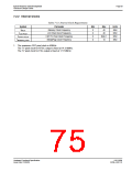
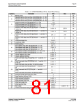
Table 7-14: EDO-DRAM Read, Write, Read-Write Timing
Symbol
Parameter
Min
25
Max
Units
ns
t1
Memory clock period
Random read or write cycle time (REG[02Bh] bits 1-0 = 00)
Random read or write cycle time (REG[02Bh] bits 1-0 = 01)
Random read or write cycle time (REG[02Bh] bits 1-0 = 10)
RAS# precharge time (REG[02Ah] bits 1-0 = 00)
5 t1
4 t1
3 t1
2 t1
1.45 t1
t1
ns
t2
t3
ns
ns
ns
RAS# precharge time (REG[02Ah] bits 1-0 = 01)
ns
RAS# precharge time (REG[02Ah] bits 1-0 = 10)
ns
RAS# to CAS# delay time (REG[02Ah] bit 4 = 0 and bits 1-0
= 00 or 10)
2 t1 - 3
t1 - 3
2 t1
ns
ns
t4
RAS# to CAS# delay time (REG[02Ah] bit 4 = 1 and bits 1-0
= 00 or 10)
t1
RAS# to CAS# delay time (REG[02Ah] bits 1-0 = 01)
CAS# precharge time
1.45 t1 - 3
0.45 t1
1.55 t1
ns
ns
ns
ns
ns
t5
t6
t7
CAS# pulse width
0.45 t1 - 1
t1
RAS# hold time
Row address setup time (REG[02Ah] bits 1-0 = 00
Row address setup time (REG[02Ah] bits 1-0 = 01)
Row address setup time (REG[02Ah] bits 1-0 = 10)
Row address hold time (REG[02Ah] bits 1-0 = 00 or 10)
Row address hold time (REG[02Ah] bits 1-0 = 01)
Column address setup time
2.45 t1 - 3
2 t1 - 3
t8
1.45 t1 - 3
0.45 t1 - 1
t1 - 3
ns
ns
ns
ns
t9
t10
t11
0.45 t1 - 3
0.45 t1 - 1
Column address hold time
Read Command setup (REG[02Ah] bit 4 = 0 and bits 1-0 =
00)
4.45 t1 - 1
2.45 t1 - 1
ns
t12
Read Command setup (REG[02Ah] bit 4 = 1 and bits 1-0 =
10)
Read Command setup (all other REG[02Ah] values)
Read Command hold (REG[02Ah] bit 4 = 0 and bits 1-0 = 00)
Read Command hold (REG[02Ah] bit 4 = 1 and bits 1-0 = 10)
Read Command hold (all other REG[02Ah] values)
Read data setup referenced from CAS#
Read data hold referenced from CAS#
Last read data setup referenced from RAS#
Bus turn-off from RAS#
3.45 t1 - 1
3.45 t1 - 1
1.45 t1 - 1
2.45 t1 - 1
4
t13
ns
t14
t15
t16
t17
t18
t19
t20
t21
t22
t23
t24
2
3
2
Write command setup time
0.45 t1 - 1
0.45 t1 - 1
0.45 t1 - 4
0.45 t1
0.45 t1
t1
ns
ns
ns
ns
ns
ns
ns
Write command hold time
Write Data setup time
Write Data hold time
MD tri-state
0.55 t1 + 19
CAS# to WE# active during read-write cycle
Write command setup during read-write cycle
1.45 t1 - 1
Last read data setup referenced from WE# during read-write
cycle
t25
t26
18
0
ns
ns
Bus tri-state from WE# during read-write cycle
t1 - 6
Hardware Functional Specification
Issue Date: 01/02/06
S1D13506
X25B-A-001-10

 EPSON [ EPSON COMPANY ]