Page 74
Epson Research and Development
Vancouver Design Center
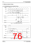
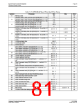
7.3.4 FPM-DRAM Read, Write, Read-Write Timing
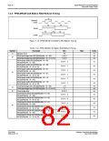
t1
Memory
Clock
t2
RAS#
t5 t6
t4
t1
t3
t8
t7
CAS#
MA
t11 t10 t11
t9
t10
R
C1
C2
C3
t12
t13
WE#(read)
MD(read)
t14
t15
d1
d2
d3
t16
t17
t20
WE#(write)
MD(write)
t18 t19
d1
d2
d3
Figure 7-16: FPM-DRAM Page Mode Timing
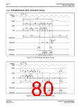
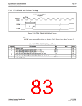
t1
Memory
Clock
RAS#
CAS#
t6
t5
t4
t1
t3
t7
t10 t11
t9
t8
MA
R
C2
C3
C1
C2
C3
C1
t12
t17
t21 t16
WE#
t14
t15
MD(read)
MD(write)
d1
d2
d3
t18 t19
t20
d1
d2
d3
Figure 7-17: FPM-DRAM Read-Write Timing
S1D13506
X25B-A-001-10
Hardware Functional Specification
Issue Date: 01/02/06

 EPSON [ EPSON COMPANY ]