Epson Research and Development
Page 67
Vancouver Design Center
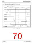
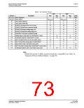
Table 7-10: Toshiba Timing
3.0V
5.0V
Symbol
Parameter
Min
Max
Min
Max
Units
MHz
ns
fDCLKOUT Clock frequency
TDCLKOUT Clock period
75
75
1/fDCLKOUT
1/fDCLKOUT
t2
t3
6
6
6
6
ns
Clock pulse width low
Clock pulse width high
ns
ns
ns
ns
ns
ns
ns
ns
ns
t4
10
0
10
0
ADDR[12:0] setup to first CLK of cycle
t5
ADDR[12:0] hold from command invalid
t6
10
5
10
5
ADDR[12:0] setup to falling edge ALE
t7
ADDR[12:0] hold from falling edge ALE
t8
0
0
CARDREG* hold from command invalid
t9
2
14
13
1
9
Falling edge of chip select to CARDxWAIT* driven
Command invalid to CARDxWAIT* tri-state
D[31:16] valid to first CLK of cycle (write cycle)
D[31:16] hold from rising edge of CARDxWAIT*
Chip select to D[31:16] driven (read cycle)
D[31:16] setup to rising edge CARDxWAIT* (read cycle)
Command invalid to D[31:16] tri-state (read cycle)
t10
t11
t12
t13
t14
t15
2
2
12
10
0
10
0
4
3
ns
ns
ns
0
0
7
30
4
16
Note
If BUSCLK exceeds 37.5MHz, it must be divided by 2 using MD12 (see Table 5-6:,
“Summary of Power-On/Reset Options,” on page 39).
Hardware Functional Specification
Issue Date: 01/02/06
S1D13506
X25B-A-001-10

 EPSON [ EPSON COMPANY ]