DS3251/DS3252/DS3253/DS3254
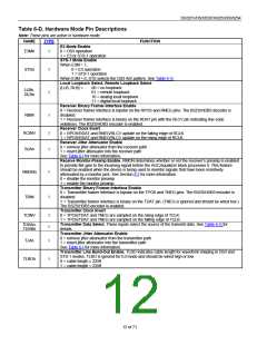
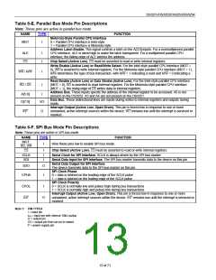
Table 6-E. Parallel Bus Mode Pin Descriptions
Note: These pins are active in parallel bus mode.
NAME
TYPE
FUNCTION
Motorola-Style Parallel CPU Interface
0 = Parallel CPU interface is Intel-style
1 = Parallel CPU interface is Motorola-style
MOT
I
Address Latch Enable. This signal controls a latch on the A[3:0] inputs. For a nonmultiplexed parallel
CPU interface, ALE is wired high to make the latch transparent. For a multiplexed parallel CPU
interface, the falling edge of ALE latches the address.
Chip Select (Active Low). CS must be asserted to read or write internal registers.
ALE
I
I
CS
Write Enable (Active Low) or Read/Write Select. For the Intel-style parallel CPU interface (MOT =
0), WR is asserted to write internal registers. For the Motorola-style parallel CPU interface (MOT = 1),
R/W determines the type of bus transaction, with R/W = 1 indicating a read and R/W = 0 indicating a
write.
I
I
WR / R/W
RD / DS
Read Enable (Active Low) or Data Strobe (Active Low). For the Intel-style parallel CPU interface
(MOT = 0), RD is asserted to read internal registers. For the Motorola-style parallel CPU interface
(MOT = 1), the rising edge of DS writes data to internal registers.
Address Bus. These inputs specify the address of the internal register to be accessed. A5 is not
present on the DS3252. A5 and A4 are not present on the DS3251.
A[5:0]
D[7:0]
I
Data Bus. These bidirectional lines are inputs during writes to internal registers and outputs during
reads.
I/O
Interrupt Output (Active Low, Open Drain). This pin is forced low in response to one or more
unmasked, active interrupt sources within the device. INT remains low until the interrupt is serviced or
masked.
INT
O
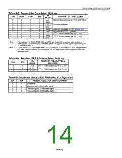
Table 6-F. SPI Bus Mode Pin Descriptions
Note: These pins are active in SPI bus mode.
NAME
TYPE
FUNCTION
MOT,
I
Wire these pins low to enable SPI bus mode.
RD, WR
I
I
I
Chip Select (Active Low). CS must be asserted to read or write internal registers.
Serial Clock for SPI Interface. SCLK is always driven by the SPI bus master.
Serial Data Input for SPI Interface. The SPI bus master transmits data to the device on this pin.
CS
SCLK
SDI
Serial Data Output for SPI Interface
SDO
O
The device transmits data to the SPI bus master on this pin.
SPI Clock Phase
CPHA
I
0 = data is latched on the leading edge of the SCLK pulse
1 = data is latched on the trailing edge of the SCLK pulse
SPI Clock Polarity
CPOL
I
0 = SCLK is normally low and pulses high during bus transactions
1 = SCLK is normally high and pulses low during bus transactions
Interrupt Output (Active Low, Open Drain). This pin is forced low in response to one or more
unmasked, active interrupt sources within the device. INT remains low until the interrupt is serviced or
masked.
INT
O
Note 1: PIN TYPES
I = input pin
IPU = input pin with internal 10kꢀ pullup
O = output pin
O3 = output pin that can be tri-stated
P = power-supply pin
13 of 71

 DALLAS [ DALLAS SEMICONDUCTOR ]